LM5642MTC National Semiconductor, LM5642MTC Datasheet - Page 6
LM5642MTC
Manufacturer Part Number
LM5642MTC
Description
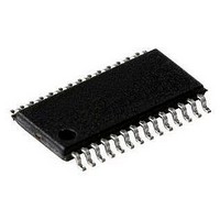
IC, DUAL SYNC BUCK CONVERTER, 28-TSSOP
Manufacturer
National Semiconductor
Datasheet
1.LM5642MTCNOPB.pdf
(28 pages)
Specifications of LM5642MTC
Primary Input Voltage
36V
No. Of Outputs
2
Output Voltage
32.4V
Output Current
20A
No. Of Pins
28
Operating Temperature Range
-40°C To +125°C
Power Dissipation Pd
1.1W
Lead Free Status / RoHS Status
Contains lead / RoHS non-compliant
Available stocks
Company
Part Number
Manufacturer
Quantity
Price

Part Number:
LM5642MTC
Manufacturer:
NS/国半
Quantity:
20 000
Part Number:
LM5642MTC/LM5642XMT
Manufacturer:
NS/国半
Quantity:
20 000
Company:
Part Number:
LM5642MTC/NOPB
Manufacturer:
NS
Quantity:
217
Part Number:
LM5642MTCX
Manufacturer:
NS/国半
Quantity:
20 000
Company:
Part Number:
LM5642MTCX/NOPB
Manufacturer:
TI
Quantity:
7 966


Note 1: Absolute maximum ratings indicate limits beyond which damage to the device may occur. Operating Range indicates conditions for which the device is
intended to be functional, but does not guarantee specfic performance limits. For guaranteed specifications and test conditions, see the Electrical Characteristics.
The guaranteed specifications apply only for the test conditions. Some performance characteristics may degrade when the device is not operated under the listed
test conditions.
Note 2: ON/SS1 and ON/SS2 are internally pulled up to one diode drop above VLIN5. Do not apply an external pull-up voltage to these pins. It may cause damage
to the IC.
)/θ
Note 3: The maximum allowable power dissipation is calculated by using P
= (T
- T
, where T
is the maximum junction temperature, T
is the
DMAX
JMAX
A
JA
JMAX
A
ambient temperature and θ
is the junction-to-ambient thermal resistance of the specified package. The power dissipation ratings results from using 125°C, 25°
JA
, and θ
respectively. A θ
C, and 90.6°C/W for T
, T
of 90.6°C/W represents the worst-case condition of no heat sinking of the 28-pin TSSOP. The eTSSOP
JMAX
A
JA
JA
package has a θ
of 29°C/W. The eTSSOP package thermal ratings results from the IC being mounted on a 4 layer JEDEC standard board using the same
JA
temperature conditions as the TSSOP package above. A thermal shutdown will occur if the temperature exceeds the maximum junction temperature of the device.
Note 4: For detailed information on soldering plastic small-outline packages, refer to the Packaging Databook available from National Semiconductor Corporation.
Note 5: For testing purposes, ESD was applied using the human-body model, a 100pF capacitor discharged through a 1.5 kΩ resistor.
Note 6: A typical is the center of characterization data measured with low duty cycle pulse tsting at T
= 25°C. Typicals are not guaranteed.
A
Note 7: All limits are guaranteed. All electrical characteristics having room-temperature limits are tested during production with T
= T
= 25°C. All hot and cold
A
J
limits are guaranteed by correlating the electrical characteristics to process and temperature variations and applying statistical process control.
Note 8: Both switching controllers are off. The linear regulator VLIN5 remains on.
Note 9: When SS1 and SS2 pins are charged above this voltage and either of the output voltages at Vout1 or Vout2 is still below the regulation limit, the under
voltage protection feature is initialized.
www.national.com
6
Related parts for LM5642MTC
Image
Part Number
Description
Manufacturer
Datasheet
Request
R

Part Number:
Description:
National Semiconductor [8-Bit D/A Converter]
Manufacturer:
National Semiconductor
Datasheet:
Part Number:
Description:
National Semiconductor [Media Coprocessor]
Manufacturer:
National Semiconductor
Datasheet:
Part Number:
Description:
Digitally Controlled Tone and Volume Circuit with Stereo Audio Power Amplifier, Microphone Preamp Stage and National 3D Sound
Manufacturer:
National Semiconductor
Datasheet:
Part Number:
Description:
Digitally Controlled Tone and Volume Circuit with Stereo Audio Power Amplifier, Microphone Preamp Stage and National 3D Sound
Manufacturer:
National Semiconductor
Datasheet:
Part Number:
Description:
AC97 Rev 2 Codec with Sample Rate Conversion and National 3D Sound
Manufacturer:
National Semiconductor
Part Number:
Description:
Manufacturer:
National Semiconductor
Datasheet:
Part Number:
Description:
Manufacturer:
National Semiconductor
Datasheet:
Part Number:
Description:
General Purpose, Low Voltage, Low Power, Rail-to-Rail Output Operational Amplifiers
Manufacturer:
National Semiconductor
Datasheet:
Part Number:
Description:
8-bit 20 MSPS flash A/D converter.
Manufacturer:
National Semiconductor
Datasheet:
Part Number:
Description:
Low Noise Quad Operational Amplifier
Manufacturer:
National Semiconductor
Datasheet:
Part Number:
Description:
Quad Differential Line Receivers
Manufacturer:
National Semiconductor
Datasheet:
Part Number:
Description:
Quad High Speed Trapezoidal? Bus Transceiver
Manufacturer:
National Semiconductor
Datasheet:
Part Number:
Description:
Dual Line Receiver
Manufacturer:
National Semiconductor
Datasheet:
Part Number:
Description:
TTL to 10k ECL Level Translator with Latch
Manufacturer:
National Semiconductor
Datasheet: