SI786LG Vishay, SI786LG Datasheet - Page 2
SI786LG
Manufacturer Part Number
SI786LG
Description
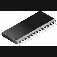
IC, DUAL POWER SUPPLY CONTROLLER, SSOP28
Manufacturer
Vishay
Datasheet
1.SI786CG.pdf
(15 pages)
Specifications of SI786LG
Primary Input Voltage
15V
No. Of Outputs
2
Output Voltage
3.3V
Output Current
25mA
No. Of Pins
28
Operating Temperature Range
-10°C To +90°C
Power Dissipation Pd
762mW
Number Of Outputs
2
Input Voltage
5.5 V to 30 V
Mounting Style
SMD/SMT
Package / Case
SSOP-28
Maximum Operating Temperature
+ 90 C
Minimum Operating Temperature
- 10 C
Lead Free Status / RoHS Status
Contains lead / RoHS non-compliant
Available stocks
Company
Part Number
Manufacturer
Quantity
Price

Part Number:
SI786LG
Manufacturer:
DG
Quantity:
20 000
Company:
Part Number:
SI786LG-T1
Manufacturer:
SILICO
Quantity:
892
Part Number:
SI786LG-T1
Manufacturer:
SI
Quantity:
20 000
Part Number:
SI786LG-T1-E3
Manufacturer:
VISHAY/威世
Quantity:
20 000
Company:
Part Number:
SI786LG-TL
Manufacturer:
VISHAY
Quantity:
2 939


Si786
Vishay Siliconix
ABSOLUTE MAXIMUM RATINGS
V+ to GND
PGND to GND
V
BST
LX
LX
Inputs/Outputs to GND
(D
SS
V
Q
DL
DH
DH
Exposure to Absolute Maximum rating conditions for extended periods may affect device reliability. Stresses above Absolute Maximum rating may cause permanent
damage. Functional operation at conditions other than the operating conditions specified is not implied. Only one Absolute Maximum rating should be applied at any one
time
www.vishay.com
2
SPECIFICATIONS
3.3-V and 5-V Step-Down Controllers
Input Supply Range
FB
FB
Load Regulation
Line Regulation
Current Limit Voltage
Current-Limit Voltage
SS
SS
SS
Internal Regulator and Reference
V
V
V
REF Output Voltage
REF Fault Lockout Voltage
REF Load Regulation
V+ Shutdown Current
V+ Standby Current
V+ Standby Current
Quiescent Power Consumption
Quiescent Power Consumption
(both PWM controllers on)
V+ Off Current
L
H
1
1
3
5
L
L
L
3
, Q
3
to GND
3
5
, D
to GND
, DL
/FB
, ON
5
3
3
3
3
3
3
to BST
to BST
Output Voltage
Fault Lockout Voltage
to LX
to LX
/SS
/SS
/SS
, BST
2
Output Voltage
Output Voltage
2
, SHDN, ON
5
to GND
5
3)
5
5
5
Switchover Voltage
p
to PGND
3
5
)
Source Current
Source Current
Fault Sink Current
5
3
5
. . . . . . . . . . . . . . . . . . . . . . . . . . . . . . . . . . . . . . . . . . .
. . . . . . . . . . . . . . . . . . . . . . . . . . . . . . . . . . . . . . . . . . . .
. . . . . . . . . . . . . . . . . . . . . . . . . . . . . . . . . . . . . .
. . . . . . . . . . . . . . . . . . . . . . . . . . . . . . . . . . . . . . . . . . .
to GND
. . . . . . . . . . . . . . . . . . . . . . . . . . . . . . . . . . . . . . . . . . .
. . . . . . . . . . . . . . . . . . . . . . . . . . . . . . . . . . . . . . . . . . .
. . . . . . . . . . . . . . . . . . . . . . . . . . . . . . . . . . . . .
. . . . . . . . . . . . . . . . . . . . . . . . . . . . . . . . . . . . .
Parameter
. . . . . . . . . . . . . . . . . . . . . . . . . . . . . . . . . . . . . . . . . . . . . .
. . . . . . . . . . . . . . . . . . . . . . . . . . . . . . . . . .
g
5
. . . . . . . . . . . . . . . . . . . . . . . . . . . . . . .
, REF, SS
. . . . . . . . . . . . . . . . . . . . . . . . . . . . . . . . . . .
5
, CS
5
. FB
5
, SYNC, CS
(includes load and line regulation)
(includes load and line regulation)
D
D
1
1
V+ = 15 V, I
Other Digital Input Levels 0 V or 5 V, T
D
0 mV < (CS
0 mV < (CS
= D
= D
1
CS
CS
= D
2
2
FB
FB
3
0 mV < (CS
6 V < V + < 30 V
= ON
= ON
Either Controller (CS_ to FB_ = 0 to 70 mV)
3
3
, FB
2
-FB
3
-0.3 V (BST
-0.3 V (BST
5
FB
-0.3 V, (V
= 0 V, FB
-0.3 V, (V
-0.3 V, (V
= CS
Rising Edge of FB
SHDN = D
= CS
ON
Either Controller (V+ = 6 V to 30 V)
5 25 V
5.25 V
3
Specific Test Conditions
3
3
(includes load and line regulation)
3
3
VL
30 V
,
3
3
= ON
= ON
or CS
or CS
Falling Edge, Hysteresis = 1%
-FB
-FB
5
-0.3 V to 36 V
-0.3 V to 20 V
= I
3
5
-0.3V to 36 V
= ON
-7 V to 0.3 V
-7 V to 0.3 V
-0.3V to 7 V
= 3.5 V
= 5.25 V, V
3
3
REF
5
) < 70 mV
) < 70 mV
H
5
5
5
L
L
-FB
5
5
0 mA < I
No External Load
0 mA < I
-FB
= 0 V, V+ =
= 0 V, V+ =
= CS
3
5
+ 0.3 V)
+ 0.3 V)
+ 0.3 V)
1
3
FB
= 0 mA, SHDN = ON
+ 0.3 )
+ 0.3 )
Falling Edge
= D
5
= 0 V, 5.5 V < V+ < 30 V
"2 V
) < 70 mV, 6 V < V + < 30 V
V+ = 30 V
5
5
5
2
=
= ON
L
L
L
5
< 25 mA
, Hysteresis = 1%
< 5 mA
Switched Over to FB
3
= ON
Si786CRG/LRG/DRG
Si786CSG/LSG/DSG
d
c
Si786DG/DRG/DSG
Si786DG/DRG/DSG
Si786DG/DRG/DSG
Si786DG/DRG/DSG
REF, V
REF Current
V
Continuous Power Dissipation (T
28-Pin SSOP
Operating Temperature Range: (T
Si786CG/CRG/CSG (C-Grade)
Si786LG/LRG/LSG (L-Grade)
Si786DG/DRG/DSG (D-Grade)
Lead Temperature (soldering, 10 sec)
Notes
a.
b.
Si786CG/LG/DG
A
L
5
= T
Current
= 0 V
3
Device mounted with all leads soldered or welded to PC board.
Derate 9.52 mW/_C above 70_C.
MIN
= ON
L
Short to GND
to T
5
. . . . . . . . . . . . . . . . . . . . . . . . . . . . . . . . . . . . . . . . . . . . . . . . .
5
= 5 V
b
MAX
. . . . . . . . . . . . . . . . . . . . . . . . . . . . . . . . . . . . . . . . . . . . . . .
. . . . . . . . . . . . . . . . . . . . . . . . . . . . . . . . . . . . . . . . . . . .
. . . . . . . . . . . . . . . . . . . . . . . . . . . . . . . . . . .
Min
4.80
3.17
3.32
3.46
3.24
. . . . . . . . . . . . . . . . . . . . . . . . . . .
5.5
2.5
2.3
4.5
3.6
4.2
2.4
80
77
2
A
. . . . . . . . . . . . . . . . . . . . . . . . . . . .
. . . . . . . . . . . . . . . . . . . . . . . . .
MIN
a
= 70_C)a
to T
. . . . . . . . . . . . . . . . . . . . . . . . . .
Limits
MAX
Typ
)
5.08
3.35
3.50
3.65
0.03
100
100
2.5
4.0
4.0
5.5
5.5
30
25
70
70
30
e
S-40807—Rev. J, 26-Apr-04
b
Document Number: 70189
Max
5.20
3.46
3.60
3.75
3.36
120
120
110
115
6.5
6.5
5.5
4.2
4.7
3.2
8.6
9.0
30
75
40
60
−10_ to 90_C
−40_ to 85_C
a
Momentary
0 to 70_C
762 mW
20 mA
50 mA
300_C
Unit
%/V
mW
mW
mV
mV
mA
mV
mA
mA
mA
mA
%
V
V
V
V
A
Related parts for SI786LG
Image
Part Number
Description
Manufacturer
Datasheet
Request
R

Part Number:
Description:
Dual-output Power-supply Controller
Manufacturer:
Vishay
Datasheet:

Part Number:
Description:
IC, BUCK, REG, 3.5A, 8HSOP
Manufacturer:
Allegro Microsystems Inc
Datasheet:

Part Number:
Description:
IC, BUCK, REG, 5.5A, 5TO220
Manufacturer:
Allegro Microsystems Inc
Datasheet:
Part Number:
Description:
357-036-542-201 CARDEDGE 36POS DL .156 BLK LOPRO
Manufacturer:
Vishay
Datasheet:
Part Number:
Description:
357-036-542-201 CARDEDGE 36POS DL .156 BLK LOPRO
Manufacturer:
Vishay
Datasheet:
Part Number:
Description:
357-036-542-201 CARDEDGE 36POS DL .156 BLK LOPRO
Manufacturer:
Vishay
Datasheet:
Part Number:
Description:
357-036-542-201 CARDEDGE 36POS DL .156 BLK LOPRO
Manufacturer:
Vishay
Datasheet:
Part Number:
Description:
357-036-542-201 CARDEDGE 36POS DL .156 BLK LOPRO
Manufacturer:
Vishay
Datasheet:
Part Number:
Description:
357-036-542-201 CARDEDGE 36POS DL .156 BLK LOPRO
Manufacturer:
Vishay
Datasheet:
Part Number:
Description:
357-036-542-201 CARDEDGE 36POS DL .156 BLK LOPRO
Manufacturer:
Vishay
Datasheet:
Part Number:
Description:
357-036-542-201 CARDEDGE 36POS DL .156 BLK LOPRO
Manufacturer:
Vishay
Datasheet:
Part Number:
Description:
357-036-542-201 CARDEDGE 36POS DL .156 BLK LOPRO
Manufacturer:
Vishay
Datasheet:
Part Number:
Description:
357-036-542-201 CARDEDGE 36POS DL .156 BLK LOPRO
Manufacturer:
Vishay
Datasheet:
Part Number:
Description:
357-036-542-201 CARDEDGE 36POS DL .156 BLK LOPRO
Manufacturer:
Vishay
Datasheet:
Part Number:
Description:
357-036-542-201 CARDEDGE 36POS DL .156 BLK LOPRO
Manufacturer:
Vishay
Datasheet: