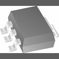
LM1117MPX-1.8 National Semiconductor, LM1117MPX-1.8 Datasheet - Page 9

LM1117MPX-1.8
Manufacturer Part Number
LM1117MPX-1.8
Description
IC, LDO VOLT REG, 1.8V, 0.8A, SOT-223-3
Manufacturer
National Semiconductor
Datasheet
1.LM1117MPX-5.0NOPB.pdf
(21 pages)
Specifications of LM1117MPX-1.8
Primary Input Voltage
15V
Output Voltage Fixed
1.8V
Dropout Voltage Vdo
1.2V
No. Of Pins
3
Output Current
800mA
Operating Temperature Range
0°C To +125°C
Termination Type
SMD
Filter Terminals
SMD
Rohs Compliant
No
Current Rating
800A
Lead Free Status / RoHS Status
Contains lead / RoHS non-compliant
Available stocks
Company
Part Number
Manufacturer
Quantity
Price
Company:
Part Number:
LM1117MPX-1.8
Manufacturer:
NATION
Quantity:
4 733
Part Number:
LM1117MPX-1.8
Manufacturer:
NS/国半
Quantity:
20 000
Part Number:
LM1117MPX-1.8(N12A)
Manufacturer:
NS/国半
Quantity:
20 000
Company:
Part Number:
LM1117MPX-1.8/NOPB
Manufacturer:
ST
Quantity:
102 650
Company:
Part Number:
LM1117MPX-1.8/NOPB
Manufacturer:
NS
Quantity:
200
Company:
Part Number:
LM1117MPX-1.8/NOPB
Manufacturer:
TI/NS
Quantity:
24 000
Part Number:
LM1117MPX-1.8/NOPB
Manufacturer:
TI/德州仪器
Quantity:
20 000
Typical Performance Characteristics
Application Note
1.0 EXTERNAL CAPACITORS/STABILITY
1.1 Input Bypass Capacitor
An input capacitor is recommended. A 10µF tantalum on the
input is a suitable input bypassing for almost all applications.
1.2 Adjust Terminal Bypass Capacitor
The adjust terminal can be bypassed to ground with a by-
pass capacitor (C
pass capacitor prevents ripple from being amplified as the
output voltage is increased. At any ripple frequency, the
impedance of the C
ripple from being amplified:
The R1 is the resistor between the output and the adjust pin.
Its value is normally in the range of 100-200Ω. For example,
with R1 = 124Ω and f
11µF.
1.3 Output Capacitor
The output capacitor is critical in maintaining regulator sta-
bility, and must meet the required conditions for both mini-
mum amount of capacitance and ESR (Equivalent Series
Resistance). The minimum output capacitance required by
the LM1117 is 10µF, if a tantalum capacitor is used. Any
increase of the output capacitance will merely improve the
loop stability and transient response. The ESR of the output
capacitor should range between 0.3Ω - 22Ω. In the case of
the adjustable regulator, when the C
output capacitance (22µf tantalum) is required.
2.0 OUTPUT VOLTAGE
The LM1117 adjustable version develops a 1.25V reference
voltage, V
As shown in Figure 1, this voltage is applied across resistor
R1 to generate a constant current I1. The current I
the adjust terminal could introduce error to the output. But
since it is very small (60µA) compared with the I1 and very
constant with line and load changes, the error can be ig-
1/(2π*f
RIPPLE
REF
LM1117-5.0 Line Transient Response
, between the output and the adjust terminal.
*C
ADJ
ADJ
ADJ
)
RIPPLE
) to improve ripple rejection. This by-
<
should be less than R1 to prevent the
R1
= 120Hz, the C
ADJ
is used, a larger
ADJ
should be
10091911
ADJ
from
>
9
(Continued)
nored. The constant current I1 then flows through the output
set resistor R2 and sets the output voltage to the desired
level.
For fixed voltage devices, R1 and R2 are integrated inside
the devices.
3.0 LOAD REGULATION
The LM1117 regulates the voltage that appears between its
output and ground pins, or between its output and adjust
pins. In some cases, line resistances can introduce errors to
the voltage across the load. To obtain the best load regula-
tion, a few precautions are needed.
Figure 2, shows a typical application using a fixed output
regulator. The Rt1 and Rt2 are the line resistances. It is
obvious that the V
the voltage drops along the line resistances. In this case, the
load regulation seen at the R
the data sheet specification. To improve this, the load should
be tied directly to the output terminal on the positive side and
directly tied to the ground terminal on the negative side.
FIGURE 1. Basic Adjustable Regulator
LOAD
is less than the V
LOAD
would be degraded from
OUT
by the sum of
www.national.com
10091917


