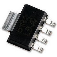
LP3852EMP-2.5/NOPB National Semiconductor, LP3852EMP-2.5/NOPB Datasheet - Page 15

LP3852EMP-2.5/NOPB
Manufacturer Part Number
LP3852EMP-2.5/NOPB
Description
IC, LDO VOLT REG, 2.5V, 1.5A, SOT-223-5
Manufacturer
National Semiconductor
Specifications of LP3852EMP-2.5/NOPB
Primary Input Voltage
7V
Output Voltage Fixed
2.5V
Dropout Voltage Vdo
240mV
No. Of Pins
5
Output Current
1.5A
Operating Temperature Range
-40°C To +125°C
Termination Type
SMD
Filter Terminals
SMD
Rohs Compliant
Yes
Lead Free Status / RoHS Status
Lead free / RoHS Compliant
Application Hints
SHUTDOWN OPERATION
A CMOS Logic level signal at the shutdown ( SD) pin will
turn-off the regulator. Pin SD must be actively terminated
through a 10kΩ pull-up resistor for a proper operation. If this
pin is driven from a source that actively pulls high and low
(such as a CMOS rail to rail comparator), the pull-up resistor
is not required. This pin must be tied to Vin if not used.
DROPOUT VOLTAGE
The dropout voltage of a regulator is defined as the minimum
input-to-output differential required to stay within 2% of the
nominal output voltage. For CMOS LDOs, the dropout volt-
age is the product of the load current and the Rds(on) of the
internal MOSFET.
REVERSE CURRENT PATH
The internal MOSFET in LP3852 and LP3855 has an inher-
ent parasitic diode. During normal operation, the input volt-
age is higher than the output voltage and the parasitic diode
is reverse biased. However, if the output is pulled above the
input in an application, then current flows from the output to
the input as the parasitic diode gets forward biased. The
output can be pulled above the input as long as the current
in the parasitic diode is limited to 200mA continuous and 1A
peak.
POWER DISSIPATION/HEATSINKING
LP3852 and LP3855 can deliver a continuous current of
1.5A over the full operating temperature range. A heatsink
may be required depending on the maximum power dissipa-
tion and maximum ambient temperature of the application.
Under all possible conditions, the junction temperature must
be within the range specified under operating conditions.
The total power dissipation of the device is given by:
P
where I
(specified under Electrical Characteristics).
D
= (V
IN
GND
−V
OUT
is the operating ground current of the device
)I
OUT
+ (V
IN
)I
GND
(Continued)
The maximum allowable temperature rise (T
on the maximum ambient temperature (T
cation, and the maximum allowable junction temperature
(T
T
The maximum allowable value for junction to ambient Ther-
mal Resistance, θ
θ
LP3852 and LP3855 are available in TO-220 and TO-263
packages. The thermal resistance depends on amount of
copper area or heat sink, and on air flow. If the maximum
allowable value of θ
TO-220 package and ≥ 60 ˚C/W for TO-263 package no
heatsink is needed since the package can dissipate enough
JA
Rmax
Jmax
= T
):
= T
Rmax
Jmax
/ P
− T
D
Amax
JA
, can be calculated using the formula:
JA
calculated above is ≥ 60 ˚C/W for
Amax
Rmax
) of the appli-
) depends


