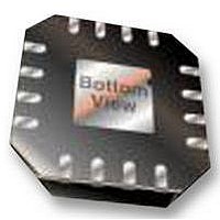
ADP322ACPZ-135 Analog Devices Inc, ADP322ACPZ-135 Datasheet - Page 15

ADP322ACPZ-135
Manufacturer Part Number
ADP322ACPZ-135
Description
IC, LDO, TRIPLE, 0.2A, 16LFCSP
Manufacturer
Analog Devices Inc
Datasheet
1.ADP322ACPZ-175-R7.pdf
(24 pages)
Specifications of ADP322ACPZ-135
Primary Input Voltage
3.8V
Output Voltage
3.3V
Dropout Voltage Vdo
110mV
No. Of Pins
16
Output Current
200mA
Voltage Regulator Case Style
LFCSP
Operating Temperature Range
-40°C To +125°C
Output Voltage Fixed
3.3V
Rohs Compliant
Yes
Lead Free Status / RoHS Status
Lead free / RoHS Compliant
Available stocks
Company
Part Number
Manufacturer
Quantity
Price
Part Number:
ADP322ACPZ-135-R7
Manufacturer:
ADI/亚德诺
Quantity:
20 000
THEORY OF OPERATION
The ADP322/ADP323 triple LDO are low quiescent current,
low dropout linear regulators that operate from 1.8 V to 5.5 V on
VIN1/VIN2 and VIN3 and provide up to 200 mA of current from
each output. Drawing a low 250 μA quiescent current (typical) at
full load makes the ADP322/ADP323 ideal for battery-operated
portable equipment. Shutdown current consumption is typically
100 nA. Optimized for use with small 1 µF ceramic capacitors,
the ADP322/ADP323 provide excellent transient performance.
VIN1/VIN2
VIN1/VIN2
VBIAS
VBIAS
VIN3
GND
VIN3
GND
EN1
EN2
EN3
EN1
EN2
EN3
VOLTAGES/CURRENTS,
VOLTAGES/CURRENTS,
Figure 43. ADP322 Internal Block Diagram
Figure 44. ADP323 Internal Block Diagram
UVLO AND THERMAL
UVLO AND THERMAL
INTERNAL BIAS
INTERNAL BIAS
SHUTDOWN
SHUTDOWN
SHUTDOWN
SHUTDOWN
SHUTDOWN
SHUTDOWN
PROTECT
PROTECT
VOUT1
VOUT2
VOUT3
VOUT1
VOUT2
VOUT3
OVERCURRENT
OVERCURRENT
OVERCURRENT
OVERCURRENT
OVERCURRENT
OVERCURRENT
0.5V
0.5V
0.5V
0.5V
REF
0.5V
REF
0.5V
REF
REF
REF
REF
+
+
+
+
–
+
–
+
–
–
–
–
VOUT1
FB1
VOUT2
FB2
VOUT3
FB3
VOUT1
VOUT2
VOUT3
Rev. 0 | Page 15 of 24
Internally, the ADP322 consists of a reference, three error
amplifiers, three feedback voltage dividers, and three PMOS
pass transistors. Output current is delivered via the PMOS pass
device, which is controlled by the error amplifier. The error
amplifier compares the reference voltage with the feedback
voltage from the output and amplifies the difference. If the
feedback voltage is lower than the reference voltage, the gate of
the PMOS device is pulled lower, allowing more current to flow
and increasing the output voltage. If the feedback voltage is
higher than the reference voltage, the gate of the PMOS device
is pulled higher, allowing less current to flow and decreasing the
output voltage.
The ADP323 is exactly the same as the ADP322 except that the
output voltage dividers are internally disconnected and the
feedback input of the error amplifiers is brought out for each
output. The output voltage can be set using the following
formula:
The value of R1 should be less than 200 kΩ to minimize errors
in the output voltage caused by the FBx pin input current. For
example, when R1 and R2 each equal 200 k Ω, the output voltage
is 1.0 V. The output voltage error introduced by the FBx pin input
current is 2 mV or 0.20%, assuming a typical FBx pin input
current of 10 nA at 25°C.
The ADP322 is available in multiple output voltage options
ranging from 0.8 V to 3.3 V.
The ADP322/ADP323 use the EN1/EN2 and EN3 pins to
enable and disable the VOUT1/VOUT2/VOUT3 pins under
normal operating conditions. When the EN1/EN2 and EN3
pins are high, VOUT1/VOUT2/VOUT3 turn on; when the
EN1/EN2 and EN3 pins are low, VOUT1/VOUT2/VOUT3 turn
off. For automatic startup, the EN1/EN2 and EN3 pins can be
tied to VBIAS.
V
OUT
= 0.5 V(1 + R1/R2) + (FB
IN
)(R1)
ADP322/ADP323


