LM2941S National Semiconductor, LM2941S Datasheet - Page 7
LM2941S
Manufacturer Part Number
LM2941S
Description
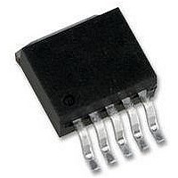
IC, ADJ LDO REG, 5V TO 20V, 1A, TO-263-5
Manufacturer
National Semiconductor
Datasheet
1.LM2941CT.pdf
(14 pages)
Specifications of LM2941S
Primary Input Voltage
26V
Output Voltage Adjustable Range
5V To 20V
Dropout Voltage Vdo
500mV
No. Of Pins
5
Output Current
1A
Operating Temperature Range
-40°C To +85°C
Lead Free Status / RoHS Status
Contains lead / RoHS non-compliant
Available stocks
Company
Part Number
Manufacturer
Quantity
Price

Part Number:
LM2941S
Manufacturer:
NS/国半
Quantity:
20 000
Company:
Part Number:
LM2941S-0.5
Manufacturer:
NS
Quantity:
3 300
Part Number:
LM2941SP+
Manufacturer:
NS/国半
Quantity:
20 000
Part Number:
LM2941SX
Manufacturer:
TI/德州仪器
Quantity:
20 000
Part Number:
LM2941SX/NOPB
Manufacturer:
TI/德州仪器
Quantity:
20 000


Definition of Terms
Dropout Voltage: The input-voltage differential at which the
circuit ceases to regulate against further reduction in input
voltage. Measured when the output voltage has dropped
100mV from the nominal value obtained at (V
dropout voltage is dependent upon load current and junction
temperature.
Input Voltage: The DC voltage applied to the input terminals
with respect to ground.
Input-Output Differential: The voltage difference between
the unregulated input voltage and the regulated output volt-
age for which the regulator will operate.
Line Regulation: The change in output voltage for a change
in the input voltage. The measurement is made under condi-
tions of low dissipation or by using pulse techniques such that
the average chip temperature is not significantly affected.
Load Regulation: The change in output voltage for a change
in load current at constant chip temperature.
Typical Applications
Note: Using 1k for R1 will ensure that the input bias current error of the adjust pin will be negligible. Do not bypass R1 or R2. This will lead to instabilities.
Maximum Power Dissipation (TO-263) (Note 4)
OUT
5V to 20V Adjustable Regulator
+ 5V) input,
7
Long Term Stability: Output voltage stability under accel-
erated life-test conditions after 1000 hours with maximum
rated voltage and junction temperature.
Output Noise Voltage: The rms AC voltage at the output,
with constant load and no input ripple, measured over a spec-
ified frequency range.
Quiescent Current: That part of the positive input current
that does not contribute to the positive load current. The reg-
ulator ground lead current.
Ripple Rejection: The ratio of the peak-to-peak input ripple
voltage to the peak-to-peak output ripple voltage.
Temperature Stability of V
output voltage for a thermal variation from room temperature
to either temperature extreme.
882329
882303
O
: The percentage change in
www.national.com
Related parts for LM2941S
Image
Part Number
Description
Manufacturer
Datasheet
Request
R

Part Number:
Description:
LM2900/LM3900/LM3301 Quad Amplifiers
Manufacturer:
National Semiconductor
Datasheet:
Part Number:
Description:
National Semiconductor [8-Bit D/A Converter]
Manufacturer:
National Semiconductor
Datasheet:
Part Number:
Description:
National Semiconductor [Media Coprocessor]
Manufacturer:
National Semiconductor
Datasheet:
Part Number:
Description:
Digitally Controlled Tone and Volume Circuit with Stereo Audio Power Amplifier, Microphone Preamp Stage and National 3D Sound
Manufacturer:
National Semiconductor
Datasheet:
Part Number:
Description:
Digitally Controlled Tone and Volume Circuit with Stereo Audio Power Amplifier, Microphone Preamp Stage and National 3D Sound
Manufacturer:
National Semiconductor
Datasheet:
Part Number:
Description:
AC97 Rev 2 Codec with Sample Rate Conversion and National 3D Sound
Manufacturer:
National Semiconductor
Part Number:
Description:
Manufacturer:
National Semiconductor
Datasheet:
Part Number:
Description:
Manufacturer:
National Semiconductor
Datasheet:
Part Number:
Description:
General Purpose, Low Voltage, Low Power, Rail-to-Rail Output Operational Amplifiers
Manufacturer:
National Semiconductor
Datasheet:
Part Number:
Description:
8-bit 20 MSPS flash A/D converter.
Manufacturer:
National Semiconductor
Datasheet:
Part Number:
Description:
Low Noise Quad Operational Amplifier
Manufacturer:
National Semiconductor
Datasheet:
Part Number:
Description:
Quad Differential Line Receivers
Manufacturer:
National Semiconductor
Datasheet:
Part Number:
Description:
Quad High Speed Trapezoidal? Bus Transceiver
Manufacturer:
National Semiconductor
Datasheet:
Part Number:
Description:
Dual Line Receiver
Manufacturer:
National Semiconductor
Datasheet: