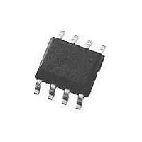
LP2986IMM-3.0 National Semiconductor, LP2986IMM-3.0 Datasheet - Page 13

LP2986IMM-3.0
Manufacturer Part Number
LP2986IMM-3.0
Description
IC, LDO VOLT REG, 3V, 0.2A, N8-SOIC
Manufacturer
National Semiconductor
Specifications of LP2986IMM-3.0
Primary Input Voltage
16V
Output Voltage Fixed
3V
Dropout Voltage Vdo
180mV
No. Of Pins
8
Output Current
200mA
Operating Temperature Range
-40°C To +125°C
Termination Type
SMD
Lead Free Status / RoHS Status
Contains lead / RoHS non-compliant
Available stocks
Company
Part Number
Manufacturer
Quantity
Price
Company:
Part Number:
LP2986IMM-3.0
Manufacturer:
NSC
Quantity:
200
Part Number:
LP2986IMM-3.0
Manufacturer:
NS/国半
Quantity:
20 000
saved by not connecting the internal divider, which means the
quiescent current is not increased by using external resistors.
A lead compensation capacitor (C
place a zero in the loop response at about 50 kHz. The value
for C
A good quality capacitor must be used for C
the value is accurate and does not change significantly over
temperature. Mica or ceramic capacitors can be used, as-
suming a tolerance of ±20% or better is selected.
If a ceramic is used, select one with a temperature coefficient
of NPO, COG, Y5P, or X7R. Capacitor types Z5U, Y5V, and
Z4V can not be used because their value varies more that
50% over the −25°C to +85°C temperature range.
SHUTDOWN INPUT OPERATION
The LP2986 is shut off by driving the Shutdown input low, and
turned on by pulling it high. If this feature is not to be used,
the Shutdown input should be tied to V
output on at all times.
To assure proper operation, the signal source used to drive
the Shutdown input must be able to swing above and below
the specified turn-on/turn-off voltage thresholds listed as V
and V
Since the Shutdown input comparator does not have hystere-
sis, It is also important that the turn-on (and turn-off) voltage
signals applied to the Shutdown input have a slew rate which
is not less than 40 mV/µs when moving between the V
V
CAUTION: The regulator output state (either On or Off) can
not be guaranteed if a slow-moving AC (or DC) signal is ap-
plied that is in the range between V
LLP MOUNTING
The LDC08A (Pullback) 8-Lead LLP package requires spe-
cific mounting techniques which are detailed in National
Semiconductor Application Note # 1187. Referring to the sec-
tion PCB Design Recommendations in AN-1187 (Page 5),
it should be noted that the pad style which should be used
with this LLP package is the NSMD (non-solder mask defined)
type. Additionally, for optimal reliability, there is a recom-
mended 1:1 ratio between the package pad and the PCB pad
for the Pullback LLP..
The thermal dissipation of the LLP package is directly related
to the printed circuit board construction and the amount of
additional copper area connected to the DAP.
The DAP (exposed pad) on the bottom of the LLP package is
connected to the die substrate with a conductive die attach
adhesive. The DAP has no direct electrical (wire) connection
to any of the eight pins. There is a parasitic PN junction be-
tween the die substrate and the device ground. As such, it is
strongly recommend that the DAP be connected directly to
the ground at device lead 1 (i.e. GROUND). Alternately, but
not recommended, the DAP may be left floating (i.e. no elec-
trical connection). The DAP must not be connected to any
potential other than ground.
For the LP2986 in the LDC08A 8-Lead LLP package, the
junction-to-case thermal rating (θ
'case' is on the bottom of the package at the center of the
DAP.
The junction-to-ambient thermal performance for the LP2986
in the LDC08A 8-Lead LLP package, using the JEDEC
JESD51 standards is summarized in the following table:
L
thresholds.
F
L
, respectively (see Electrical Characteristics).
can be found using:
C
F
= 1/(2
π
× R1 × 50k)
JC
F
H
) is 7.2°C/W, where the
) must also be used to
and V
IN
to keep the regulator
L
.
F
to ensure that
H
and
H
13
REVERSE INPUT-OUTPUT VOLTAGE
The PNP power transistor used as the pass element in the
LP2986 has an inherent diode connected between the regu-
lator output and input.
During normal operation (where the input voltage is higher
than the output) this diode is reverse-biased.
However, if the output voltage is pulled above the input, or the
input voltage is pulled below the output, this diode will turn ON
and current will flow into the regulator output pin.
In such cases, a parasitic SCR can latch which will allow a
high current to flow into V
can damage the part.
In any application where the output voltage may be higher
than the input, an external Schottky diode must be connected
from V
reverse voltage across the LP2986 to 0.3V (see the
Maximum Ratings
FIGURE 2. Adding External Schottky Diode Protection
JESD 51-3
JESD 51-7
JEDEC
2-Layer
JEDEC
4-Layer
Board
Type
IN
FIGURE 1. LP2986 Reverse Current Path
to V
OUT
(cathode on V
section.
Thermal
None
Vias
1
2
4
6
IN
(and out the ground pin), which
IN
, anode on V
7.2°C/W
7.2°C/W
7.2°C/W
7.2°C/W
7.2°C/W
θ
JC
OUT
), to limit the
www.national.com
184°C/W
1293544
64°C/W
55°C/W
46°C/W
43°C/W
1293545
θ
Absolute
JA


