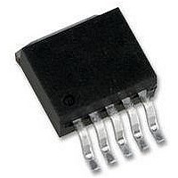
LP3962ES-3.3 National Semiconductor, LP3962ES-3.3 Datasheet - Page 15

LP3962ES-3.3
Manufacturer Part Number
LP3962ES-3.3
Description
IC, LDO VOLT REG, 3.3V, 1.5A, TO-263-5
Manufacturer
National Semiconductor
Datasheet
1.LP3962EMP-1.8.pdf
(22 pages)
Specifications of LP3962ES-3.3
Primary Input Voltage
7V
Output Voltage Fixed
3.3V
Dropout Voltage Vdo
380mV
No. Of Pins
5
Output Current
1.5A
Operating Temperature Range
-40°C To +125°C
Termination Type
SMD
Lead Free Status / RoHS Status
Contains lead / RoHS non-compliant
Available stocks
Company
Part Number
Manufacturer
Quantity
Price
Company:
Part Number:
LP3962ES-3.3
Manufacturer:
NS
Quantity:
32
Part Number:
LP3962ES-3.3
Manufacturer:
TI/德州仪器
Quantity:
20 000
Applications Information
SHUTDOWN OPERATION
A CMOS Logic level signal at the shutdown ( SD) pin will
turn-off the regulator. Pin SD must be actively terminated
through a 10kΩ pull-up resistor for a proper operation. If this
pin is driven from a source that actively pulls high and low
(such as a CMOS rail to rail comparator), the pull-up resistor
is not required. This pin must be tied to Vin if not used.
DROPOUT VOLTAGE
The dropout voltage of a regulator is defined as the minimum
input-to-output differential required to stay within 2% of the
output voltage. The LP3962/LP3965 use an internal MOS-
FET with an Rds(on) of 240mΩ (typically). For CMOS LDOs,
the dropout voltage is the product of the load current and the
Rds(on) of the internal MOSFET.
REVERSE CURRENT PATH
The internal MOSFET in LP3962and LP3965 has an inher-
ent parasitic diode. During normal operation, the input volt-
age is higher than the output voltage and the parasitic diode
is reverse biased. However, if the output is pulled above the
input in an application, then current flows from the output to
the input as the parasitic diode gets forward biased. The
output can be pulled above the input as long as the current
in the parasitic diode is limited to 200mA continuous and 1A
peak.
MAXIMUM OUTPUT CURRENT CAPABILITY
LP3962 and LP3965 can deliver a continuous current of 1.5
A over the full operating temperature range. A heatsink may
be required depending on the maximum power dissipation
and maximum ambient temperature of the application. Under
all possible conditions, the junction temperature must be
within the range specified under operating conditions. The
total power dissipation of the device is given by:
P
D
= (V
IN
−V
OUT
)I
OUT
+ (V
IN
)I
GND
FIGURE 2. Improving remote load regulation using LP3965
(Continued)
15
where I
(specified under Electrical Characteristics).
The maximum allowable temperature rise (T
on the maximum ambient temperature (T
cation, and the maximum allowable junction temperature(T
max
T
The maximum allowable value for junction to ambient Ther-
mal Resistance, θ
θ
LP3962 and LP3965 are available in TO-220, TO-263, and
SOT-223 packages. The thermal resistance depends on
amount of copper area or heat sink, and on air flow. If the
maximum allowable value of θ
˚C/W for TO-220 package, ≥60 ˚C/W for TO-263 package,
and ≥ 140 ˚C/W for SOT-223 package, no heatsink is
needed since the package can dissipate enough heat to
satisfy these requirements. If the value for allowable θ
below these limits, a heat sink is required.
HEATSINKING TO-220 PACKAGES
The thermal resistance of a TO220 package can be reduced
by attaching it to a heat sink or a copper plane on a PC
board. If a copper plane is to be used, the values of θ
be same as shown in next section for TO263 package.
The heatsink to be used in the application should have a
heatsink to ambient thermal resistance,
θ
In this equation, θ
junction to the surface of the heat sink and θ
resistance from the junction to the surface of the case. θ
about 3˚C/W for a TO220 package. The value for θ
pends on method of attachment, insulator, etc. θ
between 1.5˚C/W to 2.5˚C/W. If the exact value is unknown,
2˚C/W can be assumed.
JA
HA
Rmax
):
≤ θ
= T
= T
JA
Rmax
GND
− θ
Jmax
is the operating ground current of the device
/ P
CH
− T
D
− θ
Amax
JA
JC
CH
, can be calculated using the formula:
.
is the thermal resistance from the
JA
calculated above is ≥ 60
Amax
10126608
JC
Rmax
) of the appli-
is the thermal
www.national.com
) depends
CH
CH
JA
varies
JA
JC
falls
will
de-
is
J -


