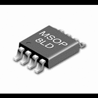
SI91822DH-AD-T1-E3 Vishay, SI91822DH-AD-T1-E3 Datasheet - Page 3

SI91822DH-AD-T1-E3
Manufacturer Part Number
SI91822DH-AD-T1-E3
Description
IC, ADJ LDO REG 1.215V TO 5V 0.3A MSOP-8
Manufacturer
Vishay
Datasheet
1.SI91822DH-12-T1.pdf
(11 pages)
Specifications of SI91822DH-AD-T1-E3
Primary Input Voltage
6V
Output Voltage Adjustable Range
1.215V To 5V
Dropout Voltage Vdo
150mV
No. Of Pins
8
Output Current
300mA
Operating Temperature Range
-40°C To +85°C
Number Of Outputs
1
Polarity
Positive
Input Voltage Max
6 V
Output Voltage
1.215 V to 5 V
Output Type
Adjustable
Dropout Voltage (max)
0.02 V at 10 mA
Line Regulation
0.18 % / V
Load Regulation
30 mV
Voltage Regulation Accuracy
1.5 %
Maximum Power Dissipation
0.846 W
Maximum Operating Temperature
+ 85 C
Mounting Style
SMD/SMT
Package / Case
MSOP-8
Minimum Operating Temperature
- 40 C
Lead Free Status / RoHS Status
Lead free / RoHS Compliant
Notes
a.
b.
c.
d.
e.
f.
g.
Document Number: 71671
S-51147—Rev. F, 20-Jun-05
SPECIFICATIONS
Dynamic Line Regulation
Dynamic Load Regulation
V
V
Thermal Shutdown
Thermal Shutdown Junction Temp
Thermal Hysteresis
Short Circuit Current
Shutdown Input
SD Input Voltage
SD Input Voltage
SD Input Current
SD Input Current
Shutdown Hysteresis
Error Output
Output High Leakage
Output Low Voltage
Out-of-Regulation Error Flag Threshold
Voltage (Rising)
Hysteresis
Delay Pin Current Source
TIMING WAVEFORMS
OUT
OUT
Room = 25_C, Full = −40 to 85_C.
The algebraic convention whereby the most negative value is a minimum and the most positive a maximum.
Typical values are for DESIGN AID ONLY, not guaranteed nor subject to production testing. Typical values for dropout voltage at V
V
Dropout voltage is defined as the input to output differential voltage at which the output voltage drops 2% below the output voltage measured with a 1-V
differential, provided that V
greater than the dropout voltage specified.
The device’s shutdown pin includes a typical 6-MW internal pull-down resistor connected to ground.
V
The Error Output (Low) function is guaranteed for V
OUT
OUT
Turn On Time
Turn-On-Time
is defined as the output voltage of the DUT at 1 mA.
= 3.3 V, while typical values for dropout voltage at V
g
Parameter
g
e
e
g
IN
does not not drop below 2.0 V. When V
Symbol
DV
DV
I
V
V
t
t
DELAY
HYST
I
J(s/d)
V
V
t
t
HYST
HYST
O(load)
I
V
OFF
V
O(line)
I
ON
ON
SC
I
IH
IL
OL
TH
IH
IL
FIGURE 4. Timing Diagram for Power-Up
IN
ERROR
w2.0 V.
0.95 V
V
V
C
C
V
OUT
OUT
V
Unless Otherwise Specified
Unless Otherwise Specified
IN
IN
IN
OUT
IN
V
V
I
OUT
V
: V
IN
IN
= 2.2 mF, C
= 2.2 mF, C
V
V
NOM
OUT
Low = Regulator OFF (Falling)
High = Regulator ON (Rising)
IN
IN
< 2 V are measured at V
= V
= V
OUT(nom)
t
R
V
V
: 1 mA to 150 mA, t
/t
= 4.3 V
= 4.3 V
SD
Test Conditions
Test Conditions
SD
= 3.3 V
OUT(nom)
OUT(nom)
F
ERROR = V
= 5 ms, I
= 0 V, Regulator OFF
= 6 V, Regulator ON
OUT(nom)
I
SINK
V
OUT
OUT
+ 1 V to V
OUT
+ 1 V, I
+ 1 V, I
t
t
= 2 mA
= 2.2 mF, V
= 2.2 mF, V
OUT
ON
DELAY
= 0 V
OUT(nom)
is less than 2.0 V, the output will be in regulation when 2.0 V − V
= 300 mA
w/o C
C
OUT(nom)
OUT
OUT
NOISE
R
/t
F
SD
SD
OUT
= 1 mA
= 1 mA
NOISE
= 2 ms
= 0.1 mF
= 1.5 V
= 1.5 V
= 1.8 V.
+ 2 V
Cap
V
NOM
Temp
Room
Room
Room
Room
Room
Room
Room
Room
Room
Room
Room
Full
Full
Full
Full
Full
Full
a
Min
0.93 x
V
1.5
1.2
OUT
b
−40 to 85_C
Vishay Siliconix
Limits
Typ
0.95 x
V
V
2% x
0.01
0.01
165
800
100
1.0
2.2
10
30
20
OUT
OUT
5
2
OUT
c
w 2 V are measured at
Max
0.97 x
V
V
0.4
0.4
3.0
OUT
2
Si91822
IN
OUT(nom)
b
www.vishay.com
Unit
mV
mV
mS
mA
mV
_C
_C
mA
mA
mA
mA
ms
is
V
V
V
V
3


