SI9182DH-AD-T1 Vishay, SI9182DH-AD-T1 Datasheet - Page 2
SI9182DH-AD-T1
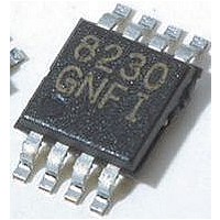
Manufacturer Part Number
SI9182DH-AD-T1
Description
IC, ADJ LDO REG, 1.5V TO 5V 250mA MSOP-8
Manufacturer
Vishay
Datasheet
1.SI9182DH-AD-T1-E3.pdf
(11 pages)
Specifications of SI9182DH-AD-T1
Primary Input Voltage
6V
Output Voltage Adjustable Range
1.5V To 5V
Dropout Voltage Vdo
105mV
No. Of Pins
8
Output Current
250mA
Operating Temperature Range
-40°C To +85°C
Number Of Outputs
1
Polarity
Positive
Input Voltage Max
6 V
Output Voltage
1.5 V to 5 V
Output Type
Adjustable
Dropout Voltage (max)
0.25 V at 200 mA
Line Regulation
0.18 % / V
Load Regulation
30 mV
Maximum Power Dissipation
0.666 W
Maximum Operating Temperature
+ 85 C
Mounting Style
SMD/SMT
Package / Case
MSOP-8
Minimum Operating Temperature
- 40 C
Lead Free Status / RoHS Status
Contains lead / RoHS non-compliant
Available stocks
Company
Part Number
Manufacturer
Quantity
Price

Part Number:
SI9182DH-AD-T1
Manufacturer:
VISHAY/威世
Quantity:
20 000
Company:
Part Number:
SI9182DH-AD-T1-E3
Manufacturer:
SILICONIX
Quantity:
2 628
Part Number:
SI9182DH-AD-T1-E3
Manufacturer:
VISHAY/威世
Quantity:
20 000


ABSOLUTE MAXIMUM RATINGS
Input Voltage, V
SD Input Voltage, V
Output Current, I
Output Voltage, V
Maximum Junction Temperature, T
Storage Temperature, T
ESD (Human Body Model)
Stresses beyond those listed under “Absolute Maximum Ratings” may cause permanent damage to the device. These are stress ratings only, and functional operation
of the device at these or any other conditions beyond those indicated in the operational sections of the specifications is not implied. Exposure to absolute maximum rating
conditions for extended periods may affect device reliability.
RECOMMENDED OPERATING RANGE
Input Voltage, V
Output Voltage, V
SD Input Voltage, V
C
C
C
www.vishay.com
2
SPECIFICATIONS
Output Voltage Range
Output Voltage Accuracy
Output Voltage Accuracy
(Fixed Versions)
Feedback Voltage (ADJ Version)
Feedback Voltage (ADJ Version)
Line Regulation
(Except 5-V Version)
Line Regulation (5-V Version)
Line Regulation (ADJ Version)
Line Regulation (ADJ Version)
Dropout Voltage
Dropout Voltage
(@V
Dropout Voltage
(@V
(@V
Ground Pin Current
IN
OUT
IN
= 2.2 mF, C
w C
Range = 1 mF to 10 mF ("10%, x5R or x7R type)
OUT
OUT
OUT
OUT
w 2 V)
t 2 V, V
t 2 V, V
Parameter
OUT
IN
IN
OUT
d
d
d
d
OUT
OUT
. . . . . . . . . . . . . . . . . . . . . . . . . . . . . . . . . . . . . . . . . . . .
. . . . . . . . . . . . . . . . . . . . . . . . . . . . . . . . . . . . . . . .
IN
IN
SD
SD
= 2.2 mF (ceramic, X5R or X7R type) , C
w 2 V)
w 2 V)
. . . . . . . . . . . . . . . . . . . . . . . . . .
. . . . . . . . . . . . . . . . . . . . . . . .
(Adjustable Version)
. . . . . . . . . . . . . . . . . . . . . . . . . . . . . . . . .
. . . . . . . . . . . . . . . . . . . . . . . . . . . . . . . . . . . .
STG
. . . . . . . . . . . . . . . . . . . . . . . . . . . . . . . . . . . . .
. . . . . . . . . . . . . . . . . . . . . . . . . .
J(max)
V
V
IN
DV
V
Symbol
. . . . . . . . . . . . . . . . . . . . . . .
IN
IN
OUT
. . . . . . . . . . . . . . . . . .
V
V
V
I
V
V
− V
GND
GND
OUT
OUT
ADJ
ADJ
OUT(nom)
OUT
OUT
100
−0.3 V to V
Short Circuit Protected
C
−55_C to 150_C
NOISE
V
Unless Otherwise Specified
IN
OUT
V
O(nom)
V
V
−0.3 V to V
OUT
IN
= 2.2 mF, C
1.5 V to 5 V
From V
= 1.5 V, From V
2 V to 6 V
0 V to V
= V
= 0.1 mF (ceramic)
1 mA v I
1 mA v I
= 5 V, From V
From V
V
+ 0.3 V
Test Conditions
150_C
OUT(nom)
Adjustable Version
to V
6.5 V
2 kV
I
I
I
I
I
I
I
I
I
I
IN
I
OUT
OUT
OUT
OUT
OUT
OUT
OUT
OUT
OUT
OUT
OUT
I
IN
IN
OUT
OUT
OUT(nom)
IN
= V
OUT
OUT
= 5.5 V to 6 V
= 200 mA
= 250 mA
= 250 mA
= 200 mA
= 250 mA
= 250 mA
= 200 mA
= 200 mA
= 250 mA
= 250 mA
= 10 mA
OUT(nom)
+ 1 V, I
= 0 mA
= 2.2 mF, V
1 V I
v 250 mA
v 250 mA
IN
IN
+ 2 V
= 2.5 V to 3.5 V
= 5.5 V to 6 V
Power Dissipation (Package)
8-Pin MSOP
Thermal Impedance (Q
8-Pin MSOP
Notes
a.
b.
Operating Ambient Temperature, T
Operating Junction Temperature, T
OUT
+ 1 V
SD
Device mounted with all leads soldered or welded to PC board.
Derate 6.6 mW/_C above T
= 1 mA
1
= 1.5 V
A
b
. . . . . . . . . . . . . . . . . . . . . . . . . . . . . . . . . . . . . . . . . . . . .
. . . . . . . . . . . . . . . . . . . . . . . . . . . . . . . . . . . . . . . . . . . . .
Temp
Room
Room
Room
Room
Room
Room
Room
Room
Room
Room
Full
Full
Full
Full
Full
Full
Full
Full
Full
Full
Full
JA
)
a
a
A
= 25_C
Min
1.191
1.179
−0.18
−0.18
−0.18
−0.18
A
J
−1.5
−2.5
1.5
. . . . . . . . . . . . . . . . . . . .
. . . . . . . . . . . . . . . . . . .
b
−40 to 85_C
Vishay Siliconix
Limits
Typ
1.215
1000
1200
105
170
210
150
85
5
S-50955—Rev. H, 16-May-05
c
Document Number: 71150
Max
1.239
1.251
1500
1900
0.18
0.18
0.18
0.18
180
275
400
250
300
450
1.5
2.5
20
5
−40_C to 125_C
Si9182
−40_C to 85_C
b
% V
% V
150_C/W
666 mW
Unit
%/V
%/V
mV
mA
m
O(
O(nom)
V
V
V
)
Related parts for SI9182DH-AD-T1
Image
Part Number
Description
Manufacturer
Datasheet
Request
R

Part Number:
Description:
IC, ADJ LDO REG, 1.5V TO 5V 250mA MSOP-8
Manufacturer:
Vishay
Datasheet:

Part Number:
Description:
IC, LDO VOLT REG, 1.8V, 250mA, MSOP-8
Manufacturer:
Vishay
Datasheet:
Part Number:
Description:
IC, LDO VOLT REG, 2.8V, 250mA, MSOP-8
Manufacturer:
Vishay
Datasheet:
Part Number:
Description:
IC, LDO VOLT REG, 3.3V, 250mA, MSOP-8
Manufacturer:
Vishay
Datasheet:
Part Number:
Description:
IC, LDO VOLT REG, 2.9V, 250mA, MSOP-8
Manufacturer:
Vishay
Datasheet:
Part Number:
Description:
IC, LDO VOLT REG, 3V, 250mA, MSOP-8
Manufacturer:
Vishay
Datasheet:
Part Number:
Description:
IC, LDO VOLT REG, 5V, 250mA, MSOP-8
Manufacturer:
Vishay
Datasheet:

Part Number:
Description:
IC,VOLT REGULATOR,FIXED,+1.5V,CMOS,TSSOP,8PIN,PLASTIC
Manufacturer:
Vishay
Datasheet:
Part Number:
Description:
IC LDO REG 500MA LN 8MSOP
Manufacturer:
Vishay
Datasheet:
Part Number:
Description:
IC,VOLT REGULATOR,FIXED,+1.8V,CMOS,TSSOP,8PIN,PLASTIC
Manufacturer:
Vishay
Datasheet:
Part Number:
Description:
IC,VOLT REGULATOR,FIXED,+2.5V,CMOS,TSSOP,8PIN,PLASTIC
Manufacturer:
Vishay
Datasheet:
Part Number:
Description:
IC,VOLT REGULATOR,FIXED,+2.8V,CMOS,TSSOP,8PIN,PLASTIC
Manufacturer:
Vishay
Datasheet:
Part Number:
Description:
IC,VOLT REGULATOR,FIXED,+2.9V,CMOS,TSSOP,8PIN,PLASTIC
Manufacturer:
Vishay
Datasheet:
Part Number:
Description:
IC,VOLT REGULATOR,FIXED,+3V,CMOS,TSSOP,8PIN,PLASTIC
Manufacturer:
Vishay
Datasheet:
Part Number:
Description:
IC,VOLT REGULATOR,FIXED,+5V,CMOS,TSSOP,8PIN,PLASTIC
Manufacturer:
Vishay
Datasheet: