MXC62020MP MEMSIC, MXC62020MP Datasheet - Page 10
MXC62020MP
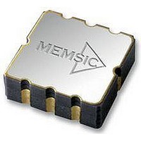
Manufacturer Part Number
MXC62020MP
Description
ACCELEROMETER, 2 AXIS, ±2.0G, I2C
Manufacturer
MEMSIC
Datasheet
1.MXC62020MP.pdf
(10 pages)
Specifications of MXC62020MP
No. Of Axes
2
Sensor Case Style
LCC
No. Of Pins
8
Supply Voltage Range
2.7V To 3.6V
Operating Temperature Range
-40°C To +85°C
Operating Temperature Max
85°C
Operating
RoHS Compliant
Acceleration Range
±2g
Available stocks
Company
Part Number
Manufacturer
Quantity
Price
Company:

Part Number:
MXC62020MP
Manufacturer:
ATT
Quantity:
5 624
Part Number:
MXC62020MP
Manufacturer:
MEMSIC
Quantity:
20 000


return from a power-down mode. The delay value depends
on the type of Memsic device. Generally speaking, low
power products tend to have longer startup time.
Fourth cycle: Master device sends a START command
followed by calling Memsic device address with a WRITE
(8
sent by Memsic device at the end.
Fifth cycle: Master device writes to Memsic device a
“[00000000]” as the starting address for which internal
memory is to be read. Since “[00000000]” is the address of
internal control register, reading from this address can serve
as a verification of operation and to confirm the write
command has been successful. Note: the starting address in
principle can be any of the 5 addresses. For example, user
can start read from address [0000001], which is X channel
MSB.
Sixth cycle: Master device calls Memsic device address
with a READ (8
device should acknowledge at the end.
addressed memory data appears on SDA line. If in step 7,
“[00000000]” was sent, internal control register data
LCC-8 PACKAGE DRAWING
MEMSIC MXC6202xG/H/M/N
Seventh cycle: Master device cycles SCL line, first
th
SCL, SDA keep low). An “acknowledge” should be
th
SCL cycle SDA line high). Memsic
Rev.C
Hermetically Sealed Package Outline
Page 10 of 10
should appear (in the following steps, this case is assumed).
Master device should send acknowledge at the end.
byte of internal memory should appear on SDA line (MSB
of X channel). The internal memory address pointer
automatically
acknowledges.
Ninth cycle: LSB of X channel. In the case that TOEN bit
of internal register was set to “1”, the MSB and LSB of
TOUT (temperature) should appear in last two steps.
Tenth cycle: MSB of Y channel.
Eleventh cycle: LSB of Y channel.
Master ends communications by sending NO acknowledge
and followed by a STOP command. Note: if mater device
continues to cycle SCL line, the memory pointer will go to
sixth
“[00000000]”. After seventh position, pointer will go to
zero again.
Optional: Master powers down Memsic device by writing
into internal control register. (See step 1 through 4 for
WRITE operation)
Eighth cycle: Master device continues cycle SCL line, next
and
seventh
moves
positions,
to
the
which
next
byte.
always
2
/26/2007
Master
have
Related parts for MXC62020MP
Image
Part Number
Description
Manufacturer
Datasheet
Request
R

Part Number:
Description:
ACCELEROMETER, 2 AXIS, ±1.7G, LCC8
Manufacturer:
MEMSIC
Datasheet:
Part Number:
Description:
ACCELEROMETER, 2 AXIS, ±1G, LCC8
Manufacturer:
MEMSIC
Datasheet:
Part Number:
Description:
ACCELEROMETER, 2 AXIS, ±1G, LCC8
Manufacturer:
MEMSIC
Datasheet:
Part Number:
Description:
ACCELEROMETER, 2 AXIS, ±1G, LCC8
Manufacturer:
MEMSIC
Datasheet:
Part Number:
Description:
ACCELEROMETER, 2 AXIS, ±2G, LCC8
Manufacturer:
MEMSIC
Datasheet:
Part Number:
Description:
ACCELEROMETER, 2 AXIS, ±1G, LCC8
Manufacturer:
MEMSIC
Datasheet:
Part Number:
Description:
ACCELEROMETER, 2 AXIS, ±2G, LCC8
Manufacturer:
MEMSIC
Datasheet:

Part Number:
Description:
IC, 3 AXIS ACCELEROMETER, ± 1.5G, LCC-16
Manufacturer:
MEMSIC
Datasheet:
Part Number:
Description:
ACCELEROMETER, 2 AXIS, ±1.7G, LCC8
Manufacturer:
MEMSIC
Datasheet:
Part Number:
Description:
ACCELEROMETER, 2 AXIS, ±10G, LCC8
Manufacturer:
MEMSIC
Datasheet:

Part Number:
Description:
Sensor, Data Acquisition Boards
Manufacturer:
memsic
Datasheet:
Part Number:
Description:
ACCELEROMETER, 2 AXIS, ±1.7G, LCC8
Manufacturer:
MEMSIC
Datasheet:
Part Number:
Description:
ACCELEROMETER, 2 AXIS, ±10G, LCC8
Manufacturer:
MEMSIC
Datasheet:
Part Number:
Description:
Sensor, Data Acquisition Boards
Manufacturer:
memsic
Datasheet:
Part Number:
Description:
Data Acquisition Board
Manufacturer:
memsic
Datasheet: