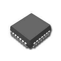
DG428DN-E3 Vishay, DG428DN-E3 Datasheet - Page 4

DG428DN-E3
Manufacturer Part Number
DG428DN-E3
Description
IC,ANALOG MUX,SINGLE,8-CHANNEL,CMOS,LDCC,20PIN,PLASTIC
Manufacturer
Vishay
Type
Analog Multiplexerr
Datasheet
1.DG428DN-E3.pdf
(12 pages)
Specifications of DG428DN-E3
Rohs Compliant
YES
Number Of Channels
8 Channel
On Resistance (max)
150 Ohms
Propagation Delay Time
250 ns
On Time (max)
300 ns
Off Time (max)
300 ns
Supply Voltage (max)
25 V
Supply Current
0.02 mA
Maximum Power Dissipation
800 mW
Maximum Operating Temperature
+ 85 C
Minimum Operating Temperature
- 40 C
Package / Case
PLCC-20
Mounting Style
SMD/SMT
Number Of Switches
Single
Package
20PLCC
Maximum On Resistance
150@12V Ohm
Maximum Propagation Delay Bus To Bus
250@±15V|280@12V ns
Maximum High Level Output Current
30 mA
Multiplexer Architecture
8:1
Maximum Turn-on Time
300@12V ns
Power Supply Type
Single|Dual
Lead Free Status / RoHS Status
Lead free / RoHS Compliant
Lead Free Status / RoHS Status
Lead free / RoHS Compliant
Available stocks
Company
Part Number
Manufacturer
Quantity
Price
Part Number:
DG428DN-E3
Manufacturer:
VISHAY/威世
Quantity:
20 000
DG428/429
Vishay Siliconix
www.vishay.com FaxBack 408-970-5600
5-4
Minimum Input Timing Requirements
Write Pulse Width
A
A
Reset Pulse Width
Power Supplies
Positive Supply Current
Negative Supply Current
Analog Switch
Analog Signal Range
Drain-Source
On-Resistance
r
Source Off
Leakage Current
Drain Off
Drain Off
Leakage Current
Drain On
Drain On
Leakage Current
Digital Control
Logic Input Current
I
Input Voltage High
Logic Input Current
Input Voltage Low
Dynamic Characteristics
Transition Time
Break-Before-Make
Interval
Enable and Write
Turn-On Time
Enable and Reset
Turn-Off Time
Charge Injection
Off Isolation
DS(on)
X
X
g
, EN Data Set Up time
, EN Data Hold Time
t V lt
Match
Parameter
p
Parameter
g
Hi h
e
Symbol
t
t
Symbol
OFF(EN, RS)
ON(EN, WR)
V
t
t
t
t
RS
I+
r
t
I–
ANALOG
W
TRANS
t
OIRR
S
H
I
I
I
I
DS(on)
r
I
OPEN
D(off)
D(off)
D(on)
D(on)
DS(on)
S(off)
I
I
I
AH
AH
AL
Q
V+ = 15 V, V– = –15 V, WR = 0, RS = 2.4
Unless Otherwise Specified
Unless Otherwise Specified
V
EN
RS = 2.4 V, V
V
V
S
V+ = 12 V, V– = 0 V, WR = 0
V
V
S
S
V
1
I
= 0 V, R
V
EN
EN
V
V
V
S
V
V
= V
C
= 0 V, 10 V, V
EN
V
= 10 V/2 V, S
V
V
V
S
Test Conditions
Test Conditions
D
S
S
V
GEN
D
= –500 A, V
V, V
V
See Figures 6 and 7
See Figures 6 and 8
L
RS = 0 V, WR = 0 V
S
EN
EN
AL
AH
= 0 V V
= 0 V, V
= 7 V
= 0 V, 10 V
= 10 V 0 V
= 10 V, 0 V
EN
= +10 V, V
= 1 nF, See Figure 9
D
= 0 V, 2.4 V, V
= 5 V, See Figure 3
0 V < V
= 0.8 V
= 2.4 V
= 2.4 V
S
See Figure 2
= 0 V, 10 V
See Figure 4
IN
See Figure 5
= 6 V, R
= 0 V
I
V
V
S
V
2.4 V
L
RMS,
A
S
S
= 2.4 V, 0.8 V
A
EN
= –1 mA
= 300
1
1
= 2.4 V
Fi
= 12 V
IN
A
A
=5 V
=5 V
S
= 0 V
= 0 RS = 5 V
= 0, RS = 5 V
= 2.4 V, 0.8 V
f = 100 kHz
< 10 V
AL
8
D
GEN
AH
= 2 V/ 10 V
= 10 V, 0 V
= 0.8 V
2
= 2.4 V
A
C
= 0
= 0 V
L
= 15 pF
f
DG428
DG429
DG428
DG429
f
Temp
Room
Room
Room
Room
Room
Room
Room
Room
Room
Room
Room
Room
Room
Temp
Full
Full
Full
Full
Full
Full
Full
Full
Full
Full
Full
Full
Full
Room
Room
Full
Full
Full
Full
b
b
Typ
160
–75
110
80
40
70
0.03
0.07
0.05
0.07
0.05
–0.001
5
4
Typ
20
c
c
Min
–100
–100
–0.5
–50
–50
–50
–55 to 125 C
–1
–1
–1
–1
–1
25
10
0
A Suffix
Min
100
100
100
–55 to 125 C
d
10
–5
A Suffix
d
Max
150
100
100
280
350
300
400
300
400
0.5
12
50
50
50
1
1
1
1
1
1
Max
100
d
d
S-52433—Rev. J, 06-Sep-99
Min
Document Number: 70063
–100
–100
–0.5
–50
–50
–50
–1
–1
–1
–1
–1
25
10
0
D Suffix
Min
–40 to 85 C
100
100
100
10
–5
d
–40 to 85 C
D Suffix
d
Max
150
100
100
280
350
300
400
300
400
0.5
12
50
50
50
Max
1
1
1
1
1
1
100
d
d
Unit
nA
pC
dB
ns
ns
%
V
A
A
A
A
A
Unit
ns
ns
A
A


