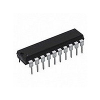
DAC0832LCN National Semiconductor, DAC0832LCN Datasheet - Page 9

DAC0832LCN
Manufacturer Part Number
DAC0832LCN
Description
D/A Converter (D-A) IC
Manufacturer
National Semiconductor
Datasheet
1.DAC0832LCN.pdf
(28 pages)
Specifications of DAC0832LCN
Resolution (bits)
8bit
Data Interface
CMOS, Parallel, TTL
No. Of Pins
20
Settling Time
1µs
Mounting Type
Through Hole
Peak Reflow Compatible (260 C)
No
No. Of Bits
8 Bit
Leaded Process Compatible
No
Number Of Channels
1
Resolution
8b
Interface Type
Parallel
Single Supply Voltage (typ)
Not RequiredV
Dual Supply Voltage (typ)
Not RequiredV
Architecture
R-2R
Power Supply Requirement
Digital
Output Type
Current
Integral Nonlinearity Error
0.2LSB
Single Supply Voltage (min)
Not RequiredV
Single Supply Voltage (max)
Not RequiredV
Dual Supply Voltage (min)
Not RequiredV
Dual Supply Voltage (max)
Not RequiredV
Operating Temp Range
0C to 70C
Operating Temperature Classification
Commercial
Mounting
Through Hole
Pin Count
20
Package Type
PDIP
Lead Free Status / RoHS Status
Contains lead / RoHS non-compliant
Lead Free Status / RoHS Status
Contains lead / RoHS non-compliant
Available stocks
Company
Part Number
Manufacturer
Quantity
Price
Company:
Part Number:
DAC0832LCN
Manufacturer:
NS
Quantity:
6 000
Company:
Part Number:
DAC0832LCN
Manufacturer:
NS
Quantity:
6 000
Part Number:
DAC0832LCN
Manufacturer:
NS/国半
Quantity:
20 000
Typical Performance Characteristics
DAC0830 Series Application Hints
These DAC’s are the industry’s first microprocessor compat-
ible, double-buffered 8-bit multiplying D to A converters.
Double-buffering allows the utmost application flexibility from
a digital control point of view. This 20-pin device is also pin
for pin compatible (with one exception) with the DAC1230, a
12-bit MICRO-DAC. In the event that a system’s analog
output resolution and accuracy must be upgraded, substitut-
ing the DAC1230 can be easily accomplished. By tying
address bit A
(double precision) which automatically increments the ad-
dress for the second byte write (starting with A
used. This allows either an 8-bit or the 12-bit part to be used
with no hardware or software changes. For the simplest 8-bit
application, this pin should be tied to V
uses in section 1.1).
Analog signal control versatility is provided by a precision
R-2R ladder network which allows full 4-quadrant multiplica-
tion of a wide range bipolar reference voltage by an applied
digital word.
1.0 DIGITAL CONSIDERATIONS
A most unique characteristic of these DAC’s is that the 8-bit
digital input byte is double-buffered. This means that the
data must transfer through two independently controlled 8-bit
latching registers before being applied to the R-2R ladder
network to change the analog output. The addition of a
second register allows two useful control features. First, any
DAC in a system can simultaneously hold the current DAC
data in one register (DAC register) and the next data word in
the second register (input register) to allow fast updating of
the DAC output on demand. Second, and probably more
important, double-buffering allows any number of DAC’s in a
system to be updated to their new analog output levels
simultaneously via a common strobe signal.
Variation vs. Supply Voltage
Gain and Linearity Error
0
to the ILE pin, a two-byte µP write instruction
00560829
CC
(also see other
0
=“1”) can be
Write Pulse Width
9
(Continued)
The timing requirements and logic level convention of the
register control signals have been designed to minimize or
eliminate external interfacing logic when applied to most
popular microprocessors and development systems. It is
easy to think of these converters as 8-bit “write-only”
memory locations that provide an analog output quantity. All
inputs to these DAC’s meet TTL voltage level specs and can
also be driven directly with high voltage CMOS logic in
non-microprocessor based systems. To prevent damage to
the chip from static discharge, all unused digital inputs
should be tied to V
are inadvertantly left floating, the DAC interprets the pin as a
logic “1”.
1.1 Double-Buffered Operation
Updating the analog output of these DAC’s in a
double-buffered manner is basically a two step or double
write operation. In a microprocessor system two unique
system addresses must be decoded, one for the input latch
controlled by the CS pin and a second for the DAC latch
which is controlled by the XFER line. If more than one DAC
is being driven, Figure 2 , the CS line of each DAC would
typically be decoded individually, but all of the converters
could share a common XFER address to allow simultaneous
updating of any number of DAC’s. The timing for this opera-
tion is shown, Figure 3 .
It is important to note that the analog outputs that will change
after a simultaneous transfer are those from the DAC’s
whose input register had been modified prior to the XFER
command.
00560830
CC
or ground. If any of the digital inputs
Data Hold Time
www.national.com
00560831


