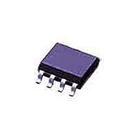
DG418BDY-E3 Vishay, DG418BDY-E3 Datasheet - Page 7

DG418BDY-E3
Manufacturer Part Number
DG418BDY-E3
Description
Improved Version Of DG418DY
Manufacturer
Vishay
Datasheet
1.DG417BDY-E3.pdf
(10 pages)
Specifications of DG418BDY-E3
Number Of Switches
Single
Switch Configuration
SPST
On Resistance (max)
35 Ohms
On Time (max)
125 ns
Off Time (max)
66 ns
Off Isolation (typ)
- 86 dB
Supply Voltage (max)
25 V
Supply Current
0.000001 mA
Maximum Power Dissipation
400 mW
Maximum Operating Temperature
+ 85 C
Mounting Style
SMD/SMT
Package / Case
SOIC-8 Narrow
Minimum Operating Temperature
- 40 C
Off State Leakage Current (max)
+/- 5 nA
Propagation Delay Time
87 ns
Switch Current (typ)
30 mA
Operating Temperature Range
-40°C To +85°C
Analog Switch Case Style
SOIC
No. Of Pins
8
Turn Off Time
80ns
Mounting Type
Surface Mount
No. Of Channels
1
Turn On Time
89ns
Rohs Compliant
Yes
Analog Switch Type
SPST
Leaded Process Compatible
Yes
Leakage Current
0.25nA
Lead Free Status / RoHS Status
Lead free / RoHS Compliant
Lead Free Status / RoHS Status
Lead free / RoHS Compliant, Lead free / RoHS Compliant
TYPICAL CHARACTERISTICS T
TEST CIRCUITS
Document Number: 72107
S09-1261-Rev. D, 13-Jul-09
V
O
is the steady state output with the switch on.
10 V
- 100
- 120
- 140
- 160
- 180
- 200
- 100
- 20
- 40
- 60
- 80
100
- 20
- 40
- 60
- 80
200
180
160
140
120
100
80
60
40
20
80
60
40
20
- 15 - 12
0
0
- 15 - 12
V+ = + 15 V
V- = - 15 V
DG417B
C
C
L
S
IN
GND
Charge Injection vs. Analog Voltage
+ 5 V
Charge Injection vs. Analog Voltage
L
= 10 nF
V
(includes fixture and stray capacitance)
L
- 9
- 9
V
O
V+ = + 12 V
V- = - 12 V
(Measured at drain pin)
(Measured at drain pin)
= V
V+ = + 12 V
V- = - 12 V
V+ = + 15 V
V- = - 15 V
- 6
- 6
S
Analog Voltage (V)
Analog Voltage (V)
- 3
+ 15 V
- 15 V
- 3
V+
V-
D
R
0
0
L
+ R
R
L
3
3
DS(on)
R
300
L
A
6
6
V+ = + 12 V
V- = 0 V
Figure 2. Switching Time (DG417B/418B)
V+ = + 12 V
V- = - 0 V
= 25 °C, unless otherwise noted
DG419B
C
L
9
9
= 10 nF
C
35 pF
12
12
L
15
V
15
O
Note:
Logic
Input
Switch
Input
Switch
Output
- 100
- 100
DG417B, DG418B, DG419B
- 20
- 40
- 60
- 80
- 20
- 40
- 60
- 80
200
180
160
140
120
100
200
180
160
140
120
100
80
60
40
20
80
60
40
20
- 15 - 12
0
0
- 15 - 12
Logic input waveform is inverted for switches that have the
opposite logic sense.
DG417B
C
DG419B
C
Charge Injection vs. Analog Voltage
L
L
Charge Injection vs. Analog Voltage
= 10 nF
3 V
0 V
0 V
= 10 nF
V
V+ = + 15 V
V- = - 15 V
S
- 9
- 9
(Measured at source pin)
(Measured at source pin)
V+ = + 15 V
V- = - 15 V
V+ = + 12 V
V- = - 12 V
V+ = + 12 V
V- = - 12 V
- 6
- 6
Analog Voltage (V)
Analog Voltage (V)
V
t
ON
O
- 3
- 3
50 %
0
0
90 %
Vishay Siliconix
3
3
V+ = + 12 V
V- = 0 V
6
6
V+ = + 12 V
V- = - 0 V
www.vishay.com
9
9
t
t
r
f
< 5 ns
< 5 ns
12
12
t
OFF
15
15
7


