DS26LV32ATMX National Semiconductor, DS26LV32ATMX Datasheet - Page 2
DS26LV32ATMX
Manufacturer Part Number
DS26LV32ATMX
Description
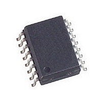
IC,LINE RECEIVER,QUAD,CMOS,DIFFERENTIAL,SOP,16PIN,PLASTIC
Manufacturer
National Semiconductor
Datasheet
1.DS26LV32ATMX.pdf
(10 pages)
Specifications of DS26LV32ATMX
Rohs Compliant
NO
Interface Circuit Standard 1
EIA/TIA-422-B/RS-422
Number Of Receivers
4
Number Of Transmitters
Not Required
Number Of Transceivers
Not Required
Data Transmission Topology
Multidrop
Receiver Signal Type
Differential
Transmitter Signal Type
Not Required
Single Supply Voltage (typ)
3.3V
Single Supply Voltage (min)
3V
Single Supply Voltage (max)
3.6V
Dual Supply Voltage (typ)
Not RequiredV
Dual Supply Voltage (min)
Not RequiredV
Dual Supply Voltage (max)
Not RequiredV
Supply Current
15mA
Power Supply Requirement
Single
Operating Temp Range
-40C to 85C
Operating Temperature Classification
Industrial
Mounting
Surface Mount
Pin Count
16
Package Type
SOIC N
Lead Free Status / Rohs Status
Not Compliant
Available stocks
Company
Part Number
Manufacturer
Quantity
Price

Part Number:
DS26LV32ATMX
Manufacturer:
TI/德州仪器
Quantity:
20 000
Company:
Part Number:
DS26LV32ATMX/NOPB
Manufacturer:
NS
Quantity:
90
Part Number:
DS26LV32ATMX/NOPB
Manufacturer:
TI/德州仪器
Quantity:
20 000


www.national.com
V
V
V
V
R
I
I
IN
EN
Symbol
TH
HY
IH
IL
IN
Absolute Maximum Ratings
If Military/Aerospace specified devices are required,
please contact the National Semiconductor Sales Office/
Distributors for availability and specifications.
Electrical Characteristics
Over Supply Voltage and Operating Temperature ranges, unless otherwise specified.
Supply Voltage (V
Enable Input Voltage (EN, EN*)
Receiver Input Voltage (V
RI−)
Receiver Input Voltage
Receiver Output Voltage (RO)
Receiver Output Current (RO)
Maximum Package Power Dissipation
Derate M Package 9.8 mW/˚C above +25˚C
(VCM: RI+, RI−)
M Package
W Package
Differential Input Threshold
Hysteresis
Minimum High Level
Input Voltage
Maximum Low Level
Input Voltage
Input Resistance
Input Current
(Other Input = 0V,
Power On, or
V
Input Current
CC
= 0V)
CC
Parameter
)
ID
: RI+,
@
±
25 mA Maximum
+25˚C
(Notes 2, 3)
V
V
V
V
+85˚C (Other Input = GND)
V
+125˚C (Other Input = GND) (Note
9)
V
V
V
V
V
V
V
V
OUT
OL
CM
IN
IN
IN
IN
IN
IN
IN
IN
IN
IN
−0.5V to +7V
−0.5V to V
−0.5V to V
= −7V, +7V, T
= −0.5V, +5.5V, T
= +10V
= +3V
= 0.5V
= −3V
= −10V
= −0.5V
= 5.5V
= 0V to V
(Note 1)
= 1.5V
1087 mW
1190 mW
= V
+0.5V
+0.5V
OH
±
±
14V
14V
Conditions
CC
CC
or
CC
A
V
+7V, T
to +85˚C
V
+5.5V, T
-55˚C to +125˚C
(Note 9)
T
+85˚C
T
+125˚C (Note 9)
2
= -40˚C to
CM
CM
A
A
A
= -40˚C to
= -55˚C to
Recommended Operating
Conditions
= -55˚C to
= −7V to
= −0.5V to
Supply Voltage (V
Operating Free Air Temperature Range (T
Derate W Package 7.3 mW/˚C above +25˚C
Storage Temperature Range
Lead Temperature Range Soldering
ESD Ratings (HBM, 1.5 k , 100 pF)
A
DS26LV32AT
DS26LV32AW
(4 Sec.)
Receiver Inputs and Enables
Other Pins
= -40˚C
A
=
RI+,
EN*
RI+,
EN*
RI−
EN,
RI−
EN,
Pin
CC
)
−200
-200
Min
2.0
5.0
5.0
0
0
0
0
0
0
Min
−40
−55
3.0
±
−0.02
−0.43
−1.26
0.27
Typ
Typ
+25
+25
8.5
1.1
17.5
3.3
35
−65˚C to +150˚C
A
+125
Max
+85
3.6
)
+200
+200
Max
−2.2
-1.8
0.8
1.8
1.8
±
1
+260˚C
Units
6.5 kV
˚C
˚C
V
2 kV
Units
mV
mV
mV
mA
mA
mA
mA
mA
mA
mA
k
k
µA
V
V
Related parts for DS26LV32ATMX
Image
Part Number
Description
Manufacturer
Datasheet
Request
R

Part Number:
Description:
3V Enhanced CMOS Quad Differential Line Receiver
Manufacturer:
National Semiconductor
Datasheet:
Part Number:
Description:
National Semiconductor [8-Bit D/A Converter]
Manufacturer:
National Semiconductor
Datasheet:
Part Number:
Description:
National Semiconductor [Media Coprocessor]
Manufacturer:
National Semiconductor
Datasheet:
Part Number:
Description:
Digitally Controlled Tone and Volume Circuit with Stereo Audio Power Amplifier, Microphone Preamp Stage and National 3D Sound
Manufacturer:
National Semiconductor
Datasheet:
Part Number:
Description:
Digitally Controlled Tone and Volume Circuit with Stereo Audio Power Amplifier, Microphone Preamp Stage and National 3D Sound
Manufacturer:
National Semiconductor
Datasheet:
Part Number:
Description:
AC97 Rev 2 Codec with Sample Rate Conversion and National 3D Sound
Manufacturer:
National Semiconductor
Part Number:
Description:
Manufacturer:
National Semiconductor
Datasheet:
Part Number:
Description:
Manufacturer:
National Semiconductor
Datasheet:
Part Number:
Description:
General Purpose, Low Voltage, Low Power, Rail-to-Rail Output Operational Amplifiers
Manufacturer:
National Semiconductor
Datasheet:
Part Number:
Description:
8-bit 20 MSPS flash A/D converter.
Manufacturer:
National Semiconductor
Datasheet:
Part Number:
Description:
Low Noise Quad Operational Amplifier
Manufacturer:
National Semiconductor
Datasheet:
Part Number:
Description:
Quad Differential Line Receivers
Manufacturer:
National Semiconductor
Datasheet:
Part Number:
Description:
Quad High Speed Trapezoidal? Bus Transceiver
Manufacturer:
National Semiconductor
Datasheet:
Part Number:
Description:
Dual Line Receiver
Manufacturer:
National Semiconductor
Datasheet: