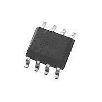
DS89C21TM National Semiconductor, DS89C21TM Datasheet - Page 2

DS89C21TM
Manufacturer Part Number
DS89C21TM
Description
Transceiver IC
Manufacturer
National Semiconductor
Datasheet
1.DS89C21TM.pdf
(6 pages)
Specifications of DS89C21TM
Device Type
Line
No. Of Drivers
1
Driver Case Style
SOIC
No. Of Pins
8
Mounting Type
Surface Mount
No. Of Driver/receivers
1/1
Peak Reflow Compatible (260 C)
No
No. Of Receivers
1
Supply Voltage
5V
Lead Free Status / RoHS Status
Contains lead / RoHS non-compliant
Available stocks
Company
Part Number
Manufacturer
Quantity
Price
Part Number:
DS89C21TM
Manufacturer:
NS/国半
Quantity:
20 000
Company:
Part Number:
DS89C21TM/NOPB
Manufacturer:
National Semiconductor
Quantity:
1 958
Company:
Part Number:
DS89C21TM/NOPB
Manufacturer:
VISHAY
Quantity:
5 485
Part Number:
DS89C21TM/NOPB
Manufacturer:
TI/德州仪器
Quantity:
20 000
Part Number:
DS89C21TMX
Manufacturer:
NS/国半
Quantity:
20 000
Company:
Part Number:
DS89C21TMX/NOPB
Manufacturer:
DM
Quantity:
6 221
www.national.com
DRIVER CHARACTERISTICS
V
V
I
V
V
V
∆V
V
V
V
∆V
I
I
RECEIVER CHARACTERISTICS
V
V
R
I
IH
OSD
OFF
IN
Symbol
IH
IL
CL
OD1
OD2
OD3
OD4
OC
TL
HYS
IN
Absolute Maximum Ratings
If Military/Aerospace specified devices are required,
please contact the National Semiconductor Sales Office/
Distributors for availability and specifications.
Electrical Characteristics
Over recommended supply voltage and operating temperature ranges, unless otherwise specified.
, I
OD2
OC
, V
IL
TH
Supply Voltage (V
Driver Input Voltage (DI)
Driver Output Voltage (DO,
DO
Receiver Input Voltage — V
CM
Differential Receiver Input
Receiver Output Voltage
(RO)
Receiver Output Current
(RO)
Storage Temperature
Range
(RI, RI
Voltage — V
*
)
Input Voltage HIGH
Input Voltage LOW
Input Current
Input Clamp Voltage
Unloaded Output Voltage
Differential Output Voltage
Change in Magnitude of V
for Complementary Output States
Differential Output Voltage
Differential Output Voltage
Common Mode Voltage
Change in Magnitude of V
for Complementary Output States
Output Short Circuit Current
Output Leakage Current
Differential Thresholds
Hysteresis
Input Impedance
Input Current
*
)
DIFF
Parameter
CC
(RI, RI
)
*
)
−1.5V to V
−0.5V to V
OD2
OC
−0.5V to +7V
(Notes 2, 3)
CC
CC
±
(Note 1)
V
I
No Load
R
R
R
R
V
V
V
V
V
Other Input = 0V,
V
V
+ 1.5V
25 mA
IN
+0.5V
CC
CC
CC
±
±
IN
L
L
L
OUT
IN
CM
IN
L
14V
14V
= −18 mA
= 100Ω
= 150Ω
= 3.9 kΩ
= 100Ω
7V
= V
= +7V, 0V, −7V
= 0V
= −7V, +7V, Other = 0V
= 5.5V and
= 0V
= 0V
= 0V
CC
, GND, 2.0V, 0.8V
2
Conditions
Recommended Operating
Conditions
Supply Voltage (V
Operating Temperature (T
Input Rise or Fall Time (DI)
V
V
V
V
V
V
V
OUT
OUT
IN
IN
IN
IN
IN
Lead Temperature (T
Maximum Junction
Temperature
Maximum Package Power Dissipation
Derate M Package
= +10V
= +3.0V
= +0.5V
= −3V
= −10V
(T
(Soldering 4 sec.)
M Package
= +6V
= −0.25V
STG
)
CC
)
L
DO,
Pin
DO*
RI,
)
A
DI
RI*
)
GND
−200
Min
−30
2.0
2.0
2.1
5.0
20
0
0
4.50
Min
−40
5.7 mW/˚C above
−65˚C to +150˚C
−0.08
+0.22
−0.04
−0.41
−1.25
−115
0.05
0.03
+1.0
Typ
±
4.2
3.0
5.0
3.1
4.0
2.0
2.0
9.5
50
25
@
Max
5.50
+85
500
+25˚C
714 mW
+260˚C
−150
+100
−100
+200
−1.5
+1.5
−2.5
Max
V
±
400
400
0.8
6.0
6.0
3.0
+25˚C
150˚C
CC
10
Units
˚C
ns
V
Units
mV
mV
mA
mV
mV
mA
mA
mA
mA
mA
kΩ
µA
µA
µA
V
V
V
V
V
V
V
V


