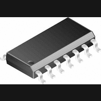
LM10CWM National Semiconductor, LM10CWM Datasheet - Page 2

LM10CWM
Manufacturer Part Number
LM10CWM
Description
Operational Amplifier (Op-Amp) IC
Manufacturer
National Semiconductor
Specifications of LM10CWM
No. Of Amplifiers
1
Slew Rate
0.2V/µs
No. Of Pins
14
Mounting Type
Surface Mount
Peak Reflow Compatible (260 C)
No
Input Bias Current
30nA
Supply Voltage
48V
Output Current
20mA
Input Offset Voltage Max
4mV
Rohs Compliant
No
Lead Free Status / RoHS Status
Contains lead / RoHS non-compliant
Available stocks
Company
Part Number
Manufacturer
Quantity
Price
Part Number:
LM10CWM
Manufacturer:
NS/国半
Quantity:
20 000
Company:
Part Number:
LM10CWMX/NOPB
Manufacturer:
2002+
Quantity:
6 221
Part Number:
LM10CWMX/NOPB
Manufacturer:
NS/国半
Quantity:
20 000
www.national.com
Input offset voltage
Input offset current
(Note 6)
Input bias current
Input resistance
Large signal voltage
gain
Shunt gain (Note 7)
Common-mode
rejection
Supply-voltage
rejection
Offset voltage drift
Offset current drift
Bias current drift
Line regulation
T
Electrical Characteristics
Absolute Maximum Ratings
If Military/Aerospace specified devices are required,
please contact the National Semiconductor Sales Office/
Distributors for availability and specifications.
Total Supply Voltage
Differential Input Voltage (Note 2)
Power Dissipation (Note 3)
Output Short-circuit Duration (Note 4)
Storage-Temp. Range
Lead Temp. (Soldering, 10 seconds)
Lead Temp. (Soldering, 10 seconds) DIP
See AN-450 “Surface Mounting Methods and Their Effect on
Product Reliability” for other methods of soldering surface
mount devices.
J
= 25˚C, T
Metal Can
Vapor Phase (60 seconds)
Infrared (15 seconds)
Parameter
MIN
T
J
T
MAX
(Boldface type refers to limits over temperature range) (Note 5)
V
V
V
I
V
V
1.2V (1.3V) V
R
0.1 mA I
1.5V V
0.1 mA I
−20V V
V
−0.2V V
V
1.0V (1.1V) V
V
T
1.2V (1.3V) V
0 I
OUT
C
S
OUT
S
S
OUT
S
+
−
L
= 1.1 k
= 1.0V (1.1V)
= −0.2V
<
=
=
=
=
REF
±
±
±
±
=
100˚C
=
=
20V, I
20V, V
0.6V (0.65V), I
20V
±
±
±
+
20 mA (
1.0 mA, V
CM
19.95V
0.4V (
−
OUT
OUT
40V, R
−39V
OUT
LM10/LM10B/ LM10BL/
Conditions
19.15V (19V)
OUT
5 mA
20 mA
±
LM10C
OUT
+
S
−55˚C to +150˚C
internally limited
±
= 0
±
0.3V), V
45V
=
L
40V
15 mA)
39.8V
40V
= 250
continuous
±
REF
19.4V
300˚C
260˚C
215˚C
220˚C
40V,
OUT
(Notes 1, 8)
= 200 mV
CM
=
LM10CL
±
= −0.4V
2 mA
±
7V
7V
2
Min
250
150
120
1.5
0.5
80
50
20
14
93
87
90
84
96
90
6
8
4
ESD rating is to be determined.
Maximum Junction Temperature
Operating Ratings
Package Thermal Resistance
LM10
LM10B
LM10C
LM10/LM10B
JA
JC
H Package
N Package
WM Package
H Package
0.001
0.25
Typ
500
400
130
102
106
0.3
3.0
2.0
2.0
10
33
25
96
60
0.003
0.006
Max
2.0
3.0
0.7
1.5
20
30
0.75
Min
150
115
1.0
80
50
25
15
10
90
87
87
84
93
90
6
6
4
LM10C
0.001
Typ
400
400
130
102
106
0.5
0.4
3.0
5.0
5.0
12
33
25
96
90
0.008
Max
0.01
4.0
5.0
2.0
3.0
30
40
150˚C/W
87˚C/W
90˚C/W
45˚C/W
150˚C
100˚C
µV/˚C
pA/˚C
pA/˚C
Units
V/mV
V/mV
V/mV
V/mV
V/mV
V/mV
V/mV
V/mV
V/mV
V/mV
85˚C
%/V
%/V
mV
mV
nA
nA
nA
nA
k
k
dB
dB
dB
dB
dB
dB


