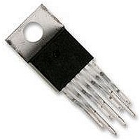
LM2676T-ADJ National Semiconductor, LM2676T-ADJ Datasheet - Page 4

LM2676T-ADJ
Manufacturer Part Number
LM2676T-ADJ
Description
DC/DC Converter IC
Manufacturer
National Semiconductor
Specifications of LM2676T-ADJ
Input Voltage
40V
Output Current
3A
Output Voltage
37V
No. Of Pins
7
Termination Type
Through Hole
Mounting Type
Through Hole
Voltage Regulator Type
Switching
Output Current Max
3A
Lead Free Status / RoHS Status
Contains lead / RoHS non-compliant
www.national.com
Symbol
DEVICE PARAMETERS
I
I
I
I
R
f
D
I
V
I
Q
STBY
CL
L
O
BIAS
ON/OFF
JA
JA
JC
JA
JA
JA
JC
Note 1: Absolute Maximum Ratings are limits beyond which damage to the device may occur. Operating Ratings indicate conditions under which of the device is
guaranteed. Operating Ratings do not imply guaranteed performance limits. For guaranteed performance limits and associated test condition, see the electrical Char-
acteristics tables.
Note 2: ESD was applied using the human-body model, a 100pF capacitor discharged through a 1.5 k
Note 3: Typical values are determined with T
Note 4: All limits are guaranteed at room temperature (standard type face) and at temperature extremes (bold type face). All room temperature limits are 100%
tested during production with T
ods. All limits are used to calculate Average Outgoing Quality Level (AOQL).
Note 5: Junction to ambient thermal resistance (no external heat sink) for the 7 lead TO-220 package mounted vertically, with
board with minimum copper area.
Note 6: Junction to ambient thermal resistance (no external heat sink) for the 7 lead TO-220 package mounted vertically, with
containing approximately 4 square inches of (1 oz.) copper area surrounding the leads.
Limits appearing in bold type face apply over the entire junction temperature range of operation, −40˚C to 125˚C.
Specifications appearing in normal type apply for T
Adjustable versions and V
ON/OFF
DS(ON)
All Output Voltage Versions
Electrical Characteristics
Quiescent
Current
Standby
Quiescent
Current
Current Limit
Output
Leakage
Current
Switch
On-Resistance
Oscillator
Frequency
Duty Cycle
Feedback Bias
Current
ON/OFF
Threshold
Voltage
ON/OFF Input
Current
Thermal
Resistance
Parameter
A
= T
IN
J
=24V for the 12V version.
= 25˚C. All limits at temperature extremes are guaranteed via correlation using standard standard Quality Control (SQC) meth-
V
For 3.3V, 5.0V, and ADJ Versions
V
For 12V Versions
ON/OFF Pin = 0V
V
V
V
I
Measured at Switch Pin
Maximum Duty Cycle
Minimum Duty Cycle
V
ADJ Version Only
ON/OFF Input = 0V
T Package, Junction to Ambient
(Note 5)
T Package, Junction to Ambient
(Note 6)
T Package, Junction to Case
S Package, Junction to Ambient
(Note 7)
S Package, Junction to Ambient
(Note 8)
S Package, Junction to Ambient
(Note 9)
S Package, Junction to Case
SWITCH
FEEDBACK
FEEDBACK
IN
SWITCH
SWITCH
FEEDBACK
= 40V, ON/OFF Pin = 0V
A
= T
= 3A
= 0V
= −1V
J
= 8V
= 15V
= 1.3V
= 25˚C and represent the most likely norm.
Conditions
A
= T
J
= 25˚C. Unless otherwise specified V
4
0.15
Typ
260
4.2
4.5
1.4
50
91
85
20
65
45
56
35
26
resistor into each pin.
1
6
0
2
2
3.8/3.6
IN
Min
225
0.8
=12V for the 3.3V, 5V and
1
1
⁄
⁄
2
2
inch leads soldered to a PC board
inch leads in a socket, or on a PC
0.17/0.29
100/150
5.25/5.4
Max
200
280
2.0
15
45
6
Units
˚C/W
kHz
mA
mA
µA
µA
nA
µA
++
%
%
A
V


