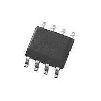
LM3477MM National Semiconductor, LM3477MM Datasheet - Page 18

LM3477MM
Manufacturer Part Number
LM3477MM
Description
Pulse Width Modulation (PWM) Controller IC
Manufacturer
National Semiconductor
Specifications of LM3477MM
Input Voltage Primary Min
2.95V
Mounting Type
Surface Mount
Topology
Buck (Step Down)
Control Mode
Current
Duty Cycle Max
93%
Input Voltage Primary Max
35V
Lead Free Status / RoHS Status
Contains lead / RoHS non-compliant
Available stocks
Company
Part Number
Manufacturer
Quantity
Price
Part Number:
LM3477MM
Manufacturer:
NS/国半
Quantity:
20 000
Part Number:
LM3477MM/NOPB
Manufacturer:
NS/国半
Quantity:
20 000
Part Number:
LM3477MMX
Manufacturer:
NS/国半
Quantity:
20 000
Company:
Part Number:
LM3477MMX/NOPB
Manufacturer:
TI
Quantity:
6 223
www.national.com
Power Mosfet Selection
MOSFET can be categorized into conduction losses and ac
switching or transition losses. R
the conduction losses. The conduction loss, P
I
is given by:
where D
The turn-on and turn-off transition times of a MOSFET from
the MOSFET specifications require tens of nano-seconds.
C
estimate the large instantaneous power loss that occurs
during these transitions.
The average amount of gate current required to turn the
MOSFET on can be calculated using the formula:
The required gate drive power to turn the MOSFET on is
equal to the switching frequency times the energy required
to deliver the charge to bring the gate charge voltage to V
(see ELECTRICAL CHARACTERISTICS and TYPICAL
PERFORMANCE CHARACTERISTICS for the drive voltage
specification).
It is sometimes helpful or necessary to slow down the turn on
transition of the FET so that less switching noise appears at
the I
R
This can help reduce sensing noise that may be preventing
designs from operating at or near the LM3477/A’s minimum
duty cycle limit. Gate drive resistors from 2.2Ω to 51Ω are
recommended.
Power Diode Selection
The output current commutates through the diode when the
external MOSFET turns off. The three most important pa-
rameters for the diode are the peak current, peak inverse
voltage, and average power dissipation. Exceeding these
ratings can cause damage to the diode. The average current
through the diode is given by:
where D is the duty cycle and I
diode must be rated to handle this current.
The off-state voltage across the diode in a buck converter is
approximately equal to the input voltage. The peak inverse
voltage rating of the diode must be greater than the off-state
voltage of the diode. To improve efficiency, a low forward
drop schottky diode is recommended.
Input Capacitor Selection
In a buck converter, the high side switch draws large ripple
currents from the input capacitor. The input capacitor must
be rated to handle this RMS current.
2
R loss across the MOSFET. The maximum conduction loss
RSS
DR
SEN
in series with the boot-strap capacitor (see Figure 6).
and Q
MAX
pin. This can be done by inserting a drive resistor
g
is the maximum operating duty cycle:
are needed from the MOSFET specifications to
I
D(AVG)
P
Drive
I
G
= I
= F
= Q
OUT
S
OUT
g
.Q
DS(ON)
.F
g
x (1-D)
S
.V
is the output current. The
DR
is needed to estimate
(Continued)
COND
, is the
DR
18
The power dissipated in the input capacitor is given by:
P
where R
capacitor must be selected to handle the rms current and
must be able to dissipate the power. P
than the rated power dissipation of the selected input capaci-
tor. In many cases, several capacitors have to be paralleled
to handle the rms current. In that case, the power dissipated
in each capacitor is given by:
P
ber of capacitors paralled at the input.
A 0.1µF or 1µF ceramic bypass capacitor is also recom-
mended on the V
be connected very close to pin 8.
Compensation
The LM3477/A is a current mode controller, therefore the
control block diagram representation involves 2 feedback
loops (see Figure 12). The inner feedback loop derives its
feedback from the sensed inductor current, while the outer
loop monitors the output voltage. This section will not give a
rigorous analysis of current mode control, but rather a sim-
plified but accurate method to determine the compensation
network. The first part reveals the results of the model, giving
expressions for solving for component values in the compen-
sation network.
The compensation network is designed around the power
components, or the power stage. An isolated schematic of
the error amplifier and the various compensation compo-
nents is shown in Figure 13. The error amplifier in conjunc-
tion with the compensation network makes up the compen-
sator block in Figure 12. The purpose of the compensator
block is to stabilize the control loop and achieve high perfor-
mance in terms of the transient response, audio susceptibil-
ity and output impedance.
FIGURE 12. Control Block Diagram of a Current Mode
D(CIN)
D(CIN)
=I
= (I
ESR_CIN
RMS_CIN
2
RMS_CIN
Controlled Buck Converter
is the ESR of the input capacitor. The input
2
IN
R
ESR_CIN
pin (pin 8) of the IC. This capacitor must
R
ESR_CIN
,
)/n
2
, where n is the total num-
D(CIN)
20003391
must be lower


