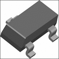
LM4040DIM3-10.0 National Semiconductor, LM4040DIM3-10.0 Datasheet - Page 23

LM4040DIM3-10.0
Manufacturer Part Number
LM4040DIM3-10.0
Description
Voltage Reference
Manufacturer
National Semiconductor
Datasheet
1.LM4040DIM3-10.0.pdf
(32 pages)
Specifications of LM4040DIM3-10.0
Reference Volt Tolerance ±%
1%
Mounting Type
Surface Mount
Voltage Regulator Type
Adjustable Shunt
Operating Temperature Max
85°C
Peak Reflow Compatible (260 C)
No
Output Current
15mA
Current Rating
15A
Fixed / Adjust / Prog
Precision
Output Voltage (max)
10V
Temperature Coefficient
40ppm/°C
Reference Voltage Accuracy (max)
1
Load Regulation
18mV
Operating Temp Range
-40C to 85C
Operating Temperature Classification
Industrial
Mounting
Surface Mount
Pin Count
3
Package Type
SOT-23
Lead Free Status / RoHS Status
Contains lead / RoHS non-compliant
Lead Free Status / RoHS Status
Contains lead / RoHS non-compliant
Electrical Characteristics(Notes)
Note 1: Absolute Maximum Ratings indicate limits beyond which damage to the device may occur. Operating Ratings indicate conditions for which the device is
functional, but do not guarantee specific performance limits. For guaranteed specifications and test conditions, see the Electrical Characteristics. The guaranteed
specifications apply only for the test conditions listed. Some performance characteristics may degrade when the device is not operated under the listed test
conditions.
Note 2: The maximum power dissipation must be derated at elevated temperatures and is dictated by T
ambient thermal resistance), and T
number given in the Absolute Maximum Ratings, whichever is lower. For the LM4040, T
is 326°C/W for the SOT-23 package, and 180°C/W with 0.4 lead length and 170°C/W with 0.125 lead length for the TO-92 package and 415°C/W for the SC70
Package.
Note 3: The human body model is a 100 pF capacitor discharged through a 1.5 kΩ resistor into each pin. The machine model is a 200 pF capacitor discharged
directly into each pin.
Note 4: Typicals are at T
Note 5: Limits are 100% production tested at 25°C. Limits over temperature are guaranteed through correlation using Statistical Quality Control (SQC) methods.
The limits are used to calculate National's AOQL.
Note 6: The boldface (over-temperature) limit for Reverse Breakdown Voltage Tolerance is defined as the room temperature Reverse Breakdown Voltage
Tolerance ±[(ΔV
of 25°C to T
range where maxΔT = 65°C is shown below:
The total over-temperature tolerance for the different grades in the exteded temperature range where max ΔT = 100 °C is shown below:
Therefore, as an example, the A-grade LM4040-2.5 has an over-temperature Reverse Breakdown Voltage tolerance of ±2.5V × 0.75% = ±19 mV.
Note 7: Load regulation is measured on pulse basis from no load to the specified load current. Output changes due to die temperature change must be taken
into account separately.
Note 8: Thermal hysteresis is defined as the difference in voltage measured at +25°C after cycling to temperature -40°C and the 25°C measurement after cycling
to temperature +125°C.
MIN
or T
R
/ΔT)(maxΔT)(V
MAX
, and V
J
= 25°C and represent most likely parametric norm.
R
R
is the reverse breakdown voltage. The total over-temperature tolerance for the different grades in the industrial temperature
)]. Where, ΔV
A
(ambient temperature). The maximum allowable power dissipation at any temperature is PD
R
/ΔT is the V
A-grade: ±0.75% = ±0.1% ±100 ppm/°C × 65°C
B-grade: ±0.85% = ±0.2% ±100 ppm/°C × 65°C
C-grade: ±1.15% = ±0.5% ±100 ppm/°C × 65°C
D-grade: ±1.98% = ±1.0% ±150 ppm/°C × 65°C
E-grade: ±2.98% = ±2.0% ±150 ppm/°C × 65°C
C-grade: ±1.5% = ±0.5% ±100 ppm/°C × 100°C
D-grade: ±2.5% = ±1.0% ±150 ppm/°C × 100°C
E-grade: ±3.5% = ±2.0% ±150 ppm/°C × 100°C
R
temperature coefficient, maxΔT is the maximum difference in temperature from the reference point
23
Jmax
= 125°C, and the typical thermal resistance (θ
Jmax
(maximum junction temperature), θ
max
= (T
JA
), when board mounted,
Jmax
− T
JA
A
www.national.com
)/θ
(junction to
JA
or the


