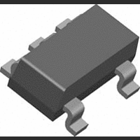
LM4120IM5-2.5 National Semiconductor, LM4120IM5-2.5 Datasheet - Page 5

LM4120IM5-2.5
Manufacturer Part Number
LM4120IM5-2.5
Description
Voltage Reference
Manufacturer
National Semiconductor
Type
Precision Micropower Low Dropout Voltage Referencer
Datasheets
1.LM4120IM5-2.5.pdf
(12 pages)
2.LM4120IM5-2.5.pdf
(11 pages)
3.LM4120IM5-2.5.pdf
(11 pages)
Specifications of LM4120IM5-2.5
Peak Reflow Compatible (260 C)
No
Leaded Process Compatible
No
Mounting Type
Surface Mount
Voltage Regulator Type
LDO Linear
Package / Case
SOT-23
Lead Free Status / RoHS Status
Contains lead / RoHS non-compliant
Available stocks
Company
Part Number
Manufacturer
Quantity
Price
Company:
Part Number:
LM4120IM5-2.5
Manufacturer:
NS
Quantity:
5 087
Part Number:
LM4120IM5-2.5
Manufacturer:
NS/国半
Quantity:
20 000
V
I
I
V
V
I
I
I
Hyst
∆V
S
SS
H
L
SC
N
H
L
Electrical Characteristics
LM4120-3.0V, 3.3V, 4.096V and 5.0V
0.01µF, T
≤ +85˚C temperature range. (Continued)
Note 1: “Absolute Maximum Ratings” indicate limits beyond which damage to the device may occur. Operating Ratings indicate conditions for which the device is
intended to be functional, but do not guarantee specific performance limits. For guaranteed specifications and test conditions, see Electrical Characteristics. The
guaranteed specifications apply only for the test conditions listed. Some performance characteristics may degrade when the device is not operated under the listed
test conditions.
Note 2: Without PCB copper enhancements. The maximum power dissipation must be de-rated at elevated temperatures and is limited by T
junction temperature), θ
= (T
Note 3: The human body model is a 100 pF capacitor discharged through a 1.5 kΩ resistor into each pin. The machine model is a 200 pF capacitor discharged
directly into each pin.
Note 4: Typical numbers are at 25˚C and represent the most likely parametric norm.
Note 5: Limits are 100% production tested at 25˚C. Limits over the operating temperature range are guaranteed through correlation using Statistical Quality Control
(SQC) methods. The limits are used to calculate National’s Averaging Outgoing Quality Level (AOQL).
Note 6: Dropout voltage is the differential voltage between V
1V for others.For 1.8V option, dropout voltage is not guaranteed over temperature. A parasitic diode exists between input and output pins; it will conduct if V
pulled to a higher voltage than V
Note 7: Thermal hysteresis is defined as the change in +25˚C output voltage before and after exposing the device to temperature extremes.
Note 8: Output noise voltage is proportional to V
Note 9: Long term stability is change in V
OUT
Symbol
JMAX
− T
A
A
= T
)/θ
J-A
j
Output Noise Voltage
(Note 8)
Supply Current
Power-down Supply
Current
Logic High Input
Voltage
Logic Low Input
Voltage
Logic High Input
Current
Logic Low Input
Current
Short Circuit Current
Thermal Hysteresis
(Note 7)
Long Term Stability
(Note 9)
= 25˚C. Limits with standard typeface are for T
up to the value listed in the Absolute Maximum Ratings.
J-A
(junction to ambient thermal resistance) and T
Parameter
IN
.
REF
at 25˚C measured continuously during 1000 hrs.
OUT
0.1 Hz to 10 Hz
10 Hz to 10 kHz
Enable = 0.4V
−40˚C ≤ T
Enable = 0.2V
V
V
−40˚C ≤ T
1000 hrs.
OUT
IN
. V
= 12V, V
N
for other voltage option is calculated using (V
= 0
OUT
J
A
@
≤ +85˚C
≤ 125˚C
and V
25˚C
Conditions
OUT
IN
= 0
A
(ambient temperature). The maximum power dissipation at any temperature is: PDiss
at which V
Unless otherwise specified V
j
5
= 25˚C, and limits in boldface type apply over the −40˚C ≤ T
OUT
changes ≤ 1% from V
Min (Note 5)
N(1.8V)
2.4
6
6
/1.8) * V
OUT
IN
at V
OUT
= V
. V
IN
Typ (Note
OUT
= 3.3V for 1.8V, 2.0V, 2.5V and V
N
160
100
(2.5V) = (36µV
2.4
0.4
0.1
0.5
20
36
15
17
4)
7
+ 1V, I
LOAD
Max (Note
PP
250
275
0.2
/1.8) * 2.5 = 46µV
15
30
30
5)
1
2
= 0, C
JMAX
www.national.com
OUT
(maximum
Units
mV/V
µV
µV
ppm
OUT
OUT
mA
µA
µA
µA
µA
=
V
V
MAX
PP
PP
PP
is
A
+
.


