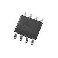
LMH6504MA National Semiconductor, LMH6504MA Datasheet - Page 12

LMH6504MA
Manufacturer Part Number
LMH6504MA
Description
Operational Amplifier (Op-Amp) IC
Manufacturer
National Semiconductor
Specifications of LMH6504MA
No. Of Amplifiers
1
No. Of Pins
8
Peak Reflow Compatible (260 C)
No
Input Bias Current
3500µA
Input Offset Voltage Max
55kV
Supply Voltage Max
12V
Leaded Process Compatible
No
Lead Free Status / RoHS Status
Contains lead / RoHS non-compliant
Available stocks
Company
Part Number
Manufacturer
Quantity
Price
Part Number:
LMH6504MA
Manufacturer:
NS/国半
Quantity:
20 000
Part Number:
LMH6504MAX
Manufacturer:
NS/国半
Quantity:
20 000
www.national.com
Application Information
GENERAL DESCRIPTION
The key features of the LMH6504 are:
Refer to Figure 1 below. The LMH6504 combines a closed
loop input buffer (“X1” Block), a voltage controlled variable
gain cell (“MULT” Block) and an output amplifier (“CFA”
Block). The input buffer is a transconductance stage whose
gain is set by the gain setting resistor, R
amplifier is a current feedback op amp and is configured as
a transimpedance stage whose gain is set by, and is equal
to, the feedback resistor, R
the LMH6504 is defined by the ratio: K · R
the gain multiplier with a nominal value of 0.965. As the gain
control input (V
adjusted over a range of about 80 dB relative to the maxi-
mum set gain.
SETTING THE LMH6504 MAXIMUM GAIN
Eq. 1
Although the LMH6504 is specified at A
recommended A
gains are possible but usually impractical due to output
offsets, noise and distortion. When varying A
tradeoffs are made:
R
R
• Low power
• Broad voltage controlled gain and attenuation range
• Bandwidth independent, resistor programmable gain
• Broad signal and gain control bandwidths
• Frequency response may be adjusted with R
• High impedance signal and gain control inputs
G
F
FIGURE 1. LMH6504 Typical Application and Block
: determines overall bandwidth
: determines the input voltage range
(From A
range (R
VMAX
G
)
G
) changes over its 0 to 2V range, the gain is
VMAX
down to complete cutoff)
varies between 2 and 100. Higher
Diagram
F
. The maximum gain, A
VMAX
F
/ R
G
G
. The output
= 9.7V/V, the
VMAX
where “K” is
F
VMAX
several
20084347
, of
12
The amount of current which the input buffer can source/sink
into R
sets the maximum input voltage:
Eq. 2
As the I
voltage or with lowering of R
tion will increase. Changes in R
on the small signal bandwidth. The output amplifier of the
LMH6504 is a current feedback amplifier (CFA) and its band-
width is determined by R
feedback resistor will roughly cut the bandwidth of the device
in half. For more about CFA’s, see the basic tutorial, OA-20,
“Current Feedback Myths Debunked”, or a more rigorous
analysis, OA-13, “Current Feedback Amplifier Loop Gain
Analysis and Performance Enhancements”.
OTHER CONFIGURATIONS
1) Single Supply Operation
The LMH6504 can be configured for use in a single supply
environment. Doing so requires the following:
a) Bias pin 4 and R
b) Ensure that V
c) Bias the input (pin 2) to make sure that it stays within the
Arranged this way, the LMH6504 will respond to the current
flowing through R
similar to the split supply arrangement with V
referenced to pin 4. Keep in mind that the circuit described
above will also center the output voltage to the “virtual half
supply voltage”.
2) Arbitrarily Referenced Input Signal
Having a wide input voltage range on the input (pin 2)
(+/-3.2V typical), the LMH6504 can be configured to control
the gain on signals which are not referenced to ground (e.g.
Half Supply biased circuits, etc.). We will call this node the
“reference node”. In such cases, the other end of R
side not tied to pin 3) can be tied to this reference node so
that R
this reference only. Keep in mind that the reference node
needs to source and sink the current flowing through R
GAIN ACCURACY
Gain accuracy is defined as the actual gain compared
against the theoretical gain at a certain V
pressed in dB) (See Figure 2).
Theoretical gain is given by:
close to the middle of V
R
capable of sinking and sourcing the expected current flow
through R
“virtual half supply”.
range of 1.8V above V
voltage Range” specification in the Electrical Character-
istics table). This can be accomplished by either DC
biasing the input and AC coupling the input signal, or
alternatively, by direct coupling if the output of the driving
stage is also biased to half supply.
G
G
G
is tied to pin 3. The “virtual half supply” needs to be
is limited and is specified in the I
will “look at” the difference between the signal and
RG_MAX
G
.
G
limit is approached (with increasing input
G
can be adjusted from 0V to 2V above the
. The gain control relationship will be
G
to a “virtual half supply” somewhere
F
. As with any CFA, doubling the
+
-
and V
G
to 1.8V below V
), the device harmonic distor-
F
will have a dramatic effect
-
range. The other end of
RG_MAX
G
+
G
(results ex-
(see “Input
spec. This
measured
G
G
(the
.


