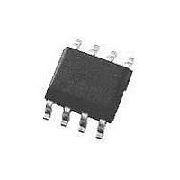
LP2995M National Semiconductor, LP2995M Datasheet

LP2995M
Specifications of LP2995M
Available stocks
Related parts for LP2995M
LP2995M Summary of contents
Page 1
... V output as a reference for the REF chipset and DDR DIMMS. Patents Pending Typical Application Circuit © 2006 National Semiconductor Corporation Features n Low output voltage offset n Works with +5v, +3.3v and 2.5v rails n Source and sink current n Low external component count ...
Page 2
... Top View Pin Descriptions SO-8 Pin or LLP Pin PSOP-8 Pin 1 1,3,4,6,9, 13 Ordering Information Order Number Package Type LP2995M LP2995MX LP2995MR LP2995MRX LP2995LQ LP2995LQX www.national.com 20039320 20039350 Name NC 2 GND 5 VSENSE 7 VREF 8 VDDQ AVIN PVIN VTT EP NSC Package Drawing SO-8 M08A ...
Page 3
... Absolute Maximum Ratings If Military/Aerospace specified devices are required, please contact the National Semiconductor Sales Office/ Distributors for availability and specifications. PVIN, AVIN, VDDQ to GND Storage Temp. Range Junction Temperature PSOP-8 Thermal Resistance (θ SO-8 Thermal Resistance (θ Electrical Characteristics type apply over the full Operating Temperature Range (T AVIN = PVIN = 2 ...
Page 4
Typical Performance Characteristics (25˚ (0, 25, 85, and 125˚ Temperature (No Load) REF www.national.com Iq vs Temperature ( V 20039309 20039311 OUT 20039313 4 = 2.5V) ...
Page 5
Typical Performance Characteristics OUT Maximum Output Current (Sinking (VDDQ = 2.5) (Continued) Maximum Output Current (Sourcing 20039315 IN 20039317 5 IN (VDDQ = 2.5) 20039316 www.national.com ...
Page 6
Block Diagram Description The LP2995 is a linear bus termination regulator designed to meet the JEDEC requirements of SSTL-2 and SSTL-3. The LP2995 is capable of sinking and sourcing current at the output V , regulating the voltage to equal ...
Page 7
Pin Descriptions AVIN AND PVIN AVIN and PVIN are the input supply pins for the LP2995. AVIN is used to supply all the internal control circuitry for the two op-amps and the output stage of V exclusively to provide the ...
Page 8
Component Selection the best solution when size and performance are critical, although their cost is typically higher than any other capaci- tor. Capacitor recommendations for different application circuits can be seen in the accompanying application notes with supporting evaluation boards. ...
Page 9
Typical Application Circuits The typical application circuit used for SSTL-2 termination schemes with DDR-SDRAM can be seen in Figure 5. For SSTL-3 and other applications it may be desirable to change internal reference voltage scaling from VDDQ * 0.5. An ...
Page 10
PCB Layout Considerations 1. AVIN and PVIN should be tied together for optimal per- formance. A local bypass capacitor should be placed as close as possible to the PVIN pin. 2. GND should be connected to a ground plane with ...
Page 11
Physical Dimensions inches (millimeters) unless otherwise noted 8-Lead Small Outline Package (M8) NS Package Number M08A 16-Lead LLP Package (LD) NS Package Number LQA16A 11 www.national.com ...
Page 12
... BANNED SUBSTANCE COMPLIANCE National Semiconductor follows the provisions of the Product Stewardship Guide for Customers (CSP-9-111C2) and Banned Substances and Materials of Interest Specification (CSP-9-111S2) for regulatory environmental compliance. Details may be found at: www.national.com/quality/green. ...


