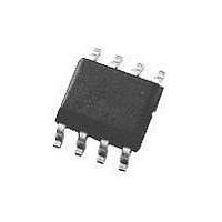
MAX660M National Semiconductor, MAX660M Datasheet - Page 6

MAX660M
Manufacturer Part Number
MAX660M
Description
DC/DC Charge Pump Converter IC
Manufacturer
National Semiconductor
Specifications of MAX660M
No. Of Pins
8
Peak Reflow Compatible (260 C)
No
Supply Voltage Max
550V
Leaded Process Compatible
No
Mounting Type
Surface Mount
Package / Case
8-SOIC
Lead Free Status / RoHS Status
Contains lead / RoHS non-compliant
Available stocks
Company
Part Number
Manufacturer
Quantity
Price
Part Number:
MAX660M
Manufacturer:
NS/国半
Quantity:
20 000
Company:
Part Number:
MAX660MJA
Manufacturer:
MAXIM
Quantity:
882
Company:
Part Number:
MAX660MJA/883B
Manufacturer:
HAR
Quantity:
23
Part Number:
MAX660MX
Manufacturer:
NS/国半
Quantity:
20 000
Company:
Part Number:
MAX660MX/NOPB
Manufacturer:
NS
Quantity:
10
Part Number:
MAX660MX/NOPB
Manufacturer:
TI/德州仪器
Quantity:
20 000
www.national.com
Application Information
Again, using a low ESR capacitor will result in lower ripple.
POSITIVE VOLTAGE DOUBLER
The MAX660 can operate as a positive voltage doubler (as
shown in the Typical Application Circuits). The doubling func-
tion is achieved by reversing some of the connections to the
device. The input voltage is applied to the GND pin with an
allowable voltage from 2.5V to 5.5V. The V+ pin is used as
the output. The LV pin and OUT pin must be connected to
ground. The OSC pin can not be driven by an external clock
in this operation mode. The unloaded output voltage is twice
of the input voltage and is not reduced by the diode D
ward drop.
The Schottky diode D
nal oscillator circuit uses the V+ pin and the LV pin (con-
nected to ground in the voltage doubler circuit) as its power
rails. Voltage across V+ and LV must be larger than 1.5V to
insure the operation of the oscillator. During start-up, D
used to charge up the voltage at V+ pin to start the oscillator;
also, it protects the device from turning-on its own parasitic
diode and potentially latching-up. Therefore, the Schottky di-
ode D
charge the output capacitor at start-up, as well as a low for-
ward voltage to prevent the internal parasitic diode from
turning-on. A Schottky diode like 1N5817 can be used for
most applications. If the input voltage ramp is less than
10V/ms, a smaller Schottky diode like MBR0520LT1 can be
used to reduce the circuit size.
SPLIT V+ IN HALF
Another interesting application shown in the Basic Applica-
tion Circuits is using the MAX660 as a precision voltage di-
vider. Since the off-voltage across each switch equals V
the input voltage can be raised to +11V.
CHANGING OSCILLATOR FREQUENCY
The internal oscillator frequency can be selected using the
Frequency Control (FC) pin. When FC is open, the oscillator
frequency is 10 kHz; when FC is connected to V+, the fre-
quency increases to 80 kHz. A higher oscillator frequency al-
1
should have enough current carrying capability to
FIGURE 3. Splitting V
1
is only needed for start-up. The inter-
IN
in Half
(Continued)
DS100898-3
1
’s for-
IN
1
/2,
is
6
lows smaller capacitors to be used for equivalent output re-
sistance and ripple, but increases the typical supply current
from 0.12 mA to 1 mA.
The oscillator frequency can be lowered by adding an exter-
nal capacitor between OSC and GND. (See Typical Perfor-
mance Characteristics.) Also, in the inverter mode, an exter-
nal clock that swings within 100 mV of V+ and GND can be
used to drive OSC. Any CMOS logic gate is suitable for driv-
ing OSC. LV must be grounded when driving OSC. The
maximum external clock frequency is limited to 150 kHz.
The switching frequency of the converter (also called the
charge pump frequency) is half of the oscillator frequency.
Note: OSC cannot be driven by an external clock in the
voltage-doubling mode.
CAPACITOR SELECTION
As discussed in the Simple Negative Voltage Converter sec-
tion, the output resistance and ripple voltage are dependent
on the capacitance and ESR values of the external capaci-
tors. The output voltage drop is the load current times the
output resistance, and the power efficiency is
Where I
and I
switch on-resistance, the two external capacitors and their
ESRs.
Since the switching current charging and discharging C
approximately twice as the output current, the effect of the
ESR of the pumping capacitor C
output resistance. The output capacitor C
discharging at a current approximately equal to the output
current, therefore, its ESR only counts once in the output re-
sistance. However, the ESR of C
voltage ripple. Therefore, low ESR capacitors ( Table 2 ) are
recommended for both capacitors to maximize efficiency, re-
duce the output voltage drop and voltage ripple. For conve-
nience, C
The output resistance varies with the oscillator frequency
and the capacitors. In Figure 4 , the output resistance vs. os-
cillator frequency curves are drawn for three different tanta-
lum capacitors. At very low frequency range, capacitance
plays the most important role in determining the output resis-
tance. Once the frequency is increased to some point (such
as 20 kHz for the 150 µF capacitors), the output resistance is
dominated by the ON resistance of the internal switches and
the ESRs of the external capacitors. A low value, smaller
size capacitor usually has a higher ESR compared with a
bigger size capacitor of the same type. For lower ESR, use
ceramic capacitors.
FC
Open
V+
Open
or V+
N/A
TABLE 1. MAX660 Oscillator Frequency Selection
L
2
R
Q
OUT
(V+) is the quiescent power loss of the IC device,
1
and C
is the conversion loss associated with the
OSC
Open
Open
External
Capacitor
External Clock
(inverter mode only)
2
are usually chosen to be the same.
1
2
is multiplied by four in the
directly affects the output
Oscillator
10 kHz
80 kHz
See Typical
Performance
Characteristics
External Clock
Frequency
2
is charging and
1
is


