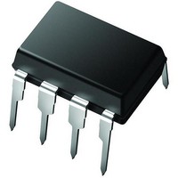
PIC12C672-10/P Microchip Technology, PIC12C672-10/P Datasheet - Page 35

PIC12C672-10/P
Manufacturer Part Number
PIC12C672-10/P
Description
IC,MICROCONTROLLER,8-BIT,PIC CPU,CMOS,DIP,8PIN,PLASTIC
Manufacturer
Microchip Technology
Series
PIC® 12Cr
Datasheets
1.PIC16F688T-ISL.pdf
(688 pages)
2.PIC12CE673-10P.pdf
(129 pages)
3.PIC12CE673-10P.pdf
(14 pages)
Specifications of PIC12C672-10/P
Rohs Compliant
YES
Core Processor
PIC
Core Size
8-Bit
Speed
10MHz
Peripherals
POR, WDT
Number Of I /o
5
Program Memory Size
3.5KB (2K x 14)
Program Memory Type
OTP
Ram Size
128 x 8
Voltage - Supply (vcc/vdd)
3 V ~ 5.5 V
Data Converters
A/D 4x8b
Oscillator Type
Internal
Operating Temperature
0°C ~ 70°C
Package / Case
8-DIP (0.300", 7.62mm)
Processor Series
PIC12C
Core
PIC
Data Bus Width
8 bit
Data Ram Size
128 B
Maximum Clock Frequency
10 MHz
Number Of Programmable I/os
5
Number Of Timers
1
Operating Supply Voltage
3 V to 5.5 V
Maximum Operating Temperature
+ 70 C
Mounting Style
Through Hole
3rd Party Development Tools
52715-96, 52716-328, 52717-734
Development Tools By Supplier
ICE2000
Minimum Operating Temperature
0 C
On-chip Adc
8 bit, 4 Channel
Lead Free Status / RoHS Status
Lead free / RoHS Compliant
For Use With
ISPICR1 - ADAPTER IN-CIRCUIT PROGRAMMINGAC124001 - MODULE SKT PROMATEII 8DIP/SOIC
Eeprom Size
-
Connectivity
-
Lead Free Status / Rohs Status
Details
FIGURE 6-3:
FIGURE 6-4:
6.2
After generating a START condition, the processor
transmits a control byte consisting of a EEPROM
address and a Read/Write bit that indicates what type
of operation is to be performed. The EEPROM address
consists of a 4-bit device code (1010) followed by three
don’t care bits.
The last bit of the control byte determines the operation
to be performed. When set to a one, a read operation
is selected, and when set to a zero, a write operation is
selected (Figure 6-5). The bus is monitored for its cor-
responding EEPROM address all the time. It generates
an acknowledge bit if the EEPROM address was true
and it is not in a programming mode.
SCL
SDA
1999 Microchip Technology Inc.
SCL
SDA
(A)
Device Addressing
CONDITION
START
(B)
Transmitter must release the SDA line at this point
allowing the Receiver to pull the SDA line low to
acknowledge the previous eight bits of data.
DATA TRANSFER SEQUENCE ON THE SERIAL BUS
ACKNOWLEDGE TIMING
1
2
3
Data from transmitter
4
ACKNOWLEDGE
ADDRESS OR
VALID
5
(C)
6
TO CHANGE
ALLOWED
7
DATA
Acknowledge
FIGURE 6-5:
8
Start Condition
Bit
S
9
1
Device Select
(D)
1
Receiver must release the SDA line at this
point so the Transmitter can continue
sending data.
0
Data from transmitter
Bits
EEPROM Address
CONTROL BYTE FORMAT
1
2
0
PIC12C67X
Acknowledge Condition
3
Read/Write Bit
X
Don’t Care
Bits
X
DS30561B-page 35
X
CONDITION
R/W
STOP
(C)
ACK
(A)


