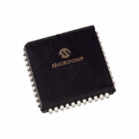
PIC18F448-I/L Microchip Technology, PIC18F448-I/L Datasheet - Page 138

PIC18F448-I/L
Manufacturer Part Number
PIC18F448-I/L
Description
IC,MICROCONTROLLER,8-BIT,PIC CPU,CMOS,LDCC,44PIN,PLASTIC
Manufacturer
Microchip Technology
Series
PIC® 18Fr
Datasheets
1.PIC18LF242-ISO.pdf
(36 pages)
2.PIC18F248-ISO.pdf
(402 pages)
3.PIC18F248-ISO.pdf
(8 pages)
Specifications of PIC18F448-I/L
Rohs Compliant
YES
Core Processor
PIC
Core Size
8-Bit
Speed
40MHz
Connectivity
CAN, I²C, SPI, UART/USART
Peripherals
Brown-out Detect/Reset, LVD, POR, PWM, WDT
Number Of I /o
33
Program Memory Size
16KB (8K x 16)
Program Memory Type
FLASH
Eeprom Size
256 x 8
Ram Size
768 x 8
Voltage - Supply (vcc/vdd)
4.2 V ~ 5.5 V
Data Converters
A/D 8x10b
Oscillator Type
External
Operating Temperature
-40°C ~ 85°C
Package / Case
44-PLCC
Processor Series
PIC18F
Core
PIC
Data Bus Width
8 bit
Data Ram Size
768 B
Interface Type
SPI, I2C, USART
Maximum Clock Frequency
40 MHz
Number Of Programmable I/os
33
Number Of Timers
4
Operating Supply Voltage
2 V to 5.5 V
Maximum Operating Temperature
+ 85 C
Mounting Style
SMD/SMT
3rd Party Development Tools
52715-96, 52716-328, 52717-734, 52712-325, EWPIC18
Development Tools By Supplier
PG164130, DV164035, DV244005, DV164005, PG164120, ICE2000, DV164136, DM163011
Minimum Operating Temperature
- 40 C
On-chip Adc
10 bit, 8 Channel
Lead Free Status / RoHS Status
Contains lead / RoHS non-compliant
For Use With
AC164309 - MODULE SKT FOR PM3 44PLCC444-1001 - DEMO BOARD FOR PICMICRO MCUDVA16XL441 - ADAPTER DEVICE ICE 44PLCCDV007003 - PROGRAMMER UNIVERSAL PROMATE II
Lead Free Status / Rohs Status
Details
Other names
PIC18F448I/L
Available stocks
Company
Part Number
Manufacturer
Quantity
Price
Company:
Part Number:
PIC18F448-I/L
Manufacturer:
Microchip Technology
Quantity:
10 000
- Current page: 138 of 402
- Download datasheet (7Mb)
16.5.2
In the Half-Bridge Output mode, two pins are used as
outputs to drive push-pull loads. The RD4/PSP4/
ECCP1/P1A pin has the PWM output signal, while the
RD5/PSP5/P1B pin has the complementary PWM
output signal (Figure 16-3). This mode can be used for
half-bridge applications, as shown in Figure 16-4, or for
full-bridge applications where four power switches are
being modulated with two PWM signals.
In Half-Bridge Output mode, the programmable dead-
band delay can be used to prevent shoot-through
current in bridge power devices. The value of register
ECCP1DEL dictates the number of clock cycles before
the output is driven active. If the value is greater than
the duty cycle, the corresponding output remains
inactive during the entire cycle. See Section 16.5.4
“Programmable Dead-Band Delay” for more details
of the dead-band delay operations.
Since the P1A and P1B outputs are multiplexed with
the PORTD<4> and PORTD<5> data latches, the
TRISD<4> and TRISD<5> bits must be cleared to
configure P1A and P1B as outputs.
FIGURE 16-4:
DS41159E-page 136
PIC18FXX8
Standard Half-Bridge Circuit (“Push-Pull”)
Half-Bridge Output Driving a Full-Bridge Circuit
HALF-BRIDGE MODE
PIC18F448/458
EXAMPLES OF HALF-BRIDGE OUTPUT MODE APPLICATIONS
P1A
P1B
PIC18F448/458
P1A
P1B
FET
Driver
FET
Driver
FET
Driver
FET
Driver
FIGURE 16-3:
+
P1A
P1B
td = Dead-Band Delay
Load
Note 1: At this time, the TMR2 register is equal to the
V+
V-
(2)
(2)
V+
V-
(1)
2: Output signals are shown as asserted high.
-
+
td
Duty Cycle
PR2 register.
Load
Period
-
td
FET
Driver
FET
Driver
HALF-BRIDGE PWM
OUTPUT
© 2006 Microchip Technology Inc.
+
V
-
+
V
-
(1)
Period
(1)
Related parts for PIC18F448-I/L
Image
Part Number
Description
Manufacturer
Datasheet
Request
R

Part Number:
Description:
IC, 8BIT MCU, PIC18F, 40MHZ, LCC-44
Manufacturer:
Microchip Technology
Datasheet:

Part Number:
Description:
IC, 8BIT MCU, PIC18LF, 40MHZ, PLCC-64
Manufacturer:
Microchip Technology
Datasheet:

Part Number:
Description:
IC, 8BIT MCU, PIC18F, 64MHZ, TQFP-80
Manufacturer:
Microchip Technology
Datasheet:

Part Number:
Description:
MCU, MPU & DSP Development Tools CAN/LIN PICtail Plus Daughter Board
Manufacturer:
Microchip Technology
Datasheet:

Part Number:
Description:
IC, 8BIT MCU, PIC18F, 64MHZ, DIP-40
Manufacturer:
Microchip Technology
Datasheet:

Part Number:
Description:
IC, 8BIT MCU, PIC18LF, 40MHZ, PLCC-64
Manufacturer:
Microchip Technology
Datasheet:

Part Number:
Description:
IC, 8BIT MCU, PIC18F, 64MHZ, TQFP-64
Manufacturer:
Microchip Technology

Part Number:
Description:
IC, 8BIT MCU, PIC18F, 64MHZ, TQFP-80
Manufacturer:
Microchip Technology

Part Number:
Description:
8KB, Flash, 768bytes-RAM, 36I/O, 8-bit Family,nanowatt XLP 40 UQFN 5x5x0.5mm TUB
Manufacturer:
Microchip Technology
Datasheet:

Part Number:
Description:
8KB, Flash, 768bytes-RAM, 36I/O, 8-bit Family,nanowatt XLP 40 UQFN 5x5x0.5mm TUB
Manufacturer:
Microchip Technology

Part Number:
Description:
16KB, Flash, 768bytes-RAM, 36I/O, 8-bit Family,nanowatt XLP 40 UQFN 5x5x0.5mm TU
Manufacturer:
Microchip Technology
Datasheet:

Part Number:
Description:
16KB, Flash, 768bytes-RAM, 36I/O, 8-bit Family,nanowatt XLP 40 UQFN 5x5x0.5mm TU
Manufacturer:
Microchip Technology

Part Number:
Description:
32KB, Flash, 1536bytes-RAM, 36I/O, 8-bit Family,nanowatt XLP 40 UQFN 5x5x0.5mm T
Manufacturer:
Microchip Technology
Datasheet:

Part Number:
Description:
32KB, Flash, 1536bytes-RAM, 36I/O, 8-bit Family,nanowatt XLP 40 UQFN 5x5x0.5mm T
Manufacturer:
Microchip Technology

Part Number:
Description:
64KB, Flash, 3968bytes-RAM, 36I/O, 8-bit Family,nanowatt XLP 40 UQFN 5x5x0.5mm T
Manufacturer:
Microchip Technology
Datasheet:


