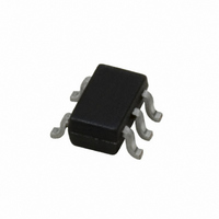
LM94021QBIMGX/NOPB National Semiconductor, LM94021QBIMGX/NOPB Datasheet - Page 10

LM94021QBIMGX/NOPB
Manufacturer Part Number
LM94021QBIMGX/NOPB
Description
TEMP SENSOR MULTI-GAIN SC70-5
Manufacturer
National Semiconductor
Series
PowerWise®r
Datasheet
1.LM94021EVAL.pdf
(14 pages)
Specifications of LM94021QBIMGX/NOPB
Sensing Temperature
-50°C ~ 150°C
Output Type
Voltage
Voltage - Supply
1.5 V ~ 5.5 V
Accuracy
±2.7°C
Package / Case
6-TSSOP (5 lead), SC-88A, SOT-353
Lead Free Status / RoHS Status
Lead free / RoHS Compliant
Other names
LM94021QBIMGX
www.national.com
4.0 CAPACITIVE LOADS
The LM94021 handles capacitive loading well. In an extreme-
ly noisy environment, or when driving a switched sampling
input on an ADC, it may be necessary to add some filtering to
minimize noise coupling. Without any precautions, the
LM94021 can drive a capacitive load less than or equal to
1100 pF as shown in
than 1100 pF, a series resistor may be required on the output,
as shown in
FIGURE 3. LM94021 with Series Resistor for Capacitive
FIGURE 2. LM94021 No Decoupling Required for
Capacitive Loads Less than 1100 pF
1.1 nF to 99 nF
100 nF to 999 nF
1 μF
Figure
Loading greater than 1100 pF
3.
C
LOAD
Figure
2. For capacitive loads greater
3 kΩ
1.5 kΩ
800 Ω
R
S
20108615
20108633
10
5.0 OUTPUT VOLTAGE SHIFT
The LM94021 is very linear over temperature and supply volt-
age range. Due to the intrinsic behavior of an NMOS/PMOS
rail-to-rail buffer, a slight shift in the output can occur when
the supply voltage is ramped over the operating range of the
device. The location of the shift is determined by the relative
levels of V
V
This slight shift (a few millivolts) takes place over a wide
change (approximately 200 mV) in V
shift takes place over a wide temperature change of 5°C to
20°C, V
in the Electrical Characteristics table already include this pos-
sible shift.
6.0 SELECTABLE GAIN FOR OPTIMIZATION AND IN SITU
TESTING
The Gain Select digital inputs can be tied to the rails or can
be driven from digital outputs such as microcontroller GPIO
pins. In low-supply voltage applications, the ability to reduce
the gain to −5.5 mV/°C allows the LM94021 to operate over
the full −50°C to 150°C range. When a larger supply voltage
is present, the gain can be increased as high as
−13.6 mV/°C. The larger gain is optimal for reducing the ef-
fects of noise (for example, noise coupling on the output line
or quantization noise induced by an analog-to-digital convert-
er which may be sampling the LM94021 output).
Another application advantage of the digitally selectable gain
is the ability to perform dynamic testing of the LM94021 while
it is running in a system. By toggling the logic levels of the
gain select pins and monitoring the resultant change in the
output voltage level, the host system can verify the function-
ality of the LM94021.
DD
- V
OUT
OUT
= 1.0V.
is always monotonic. The accuracy specifications
DD
and V
OUT
. The shift typically occurs when
DD
or V
OUT
. Since the


