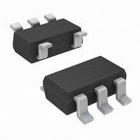
TC6501P125VCTRTG Microchip Technology, TC6501P125VCTRTG Datasheet - Page 2

TC6501P125VCTRTG
Manufacturer Part Number
TC6501P125VCTRTG
Description
IC TEMP SWTCH OPEN DRAIN SOT23A5
Manufacturer
Microchip Technology
Datasheet
1.TC6504P005VCTTR.pdf
(17 pages)
Specifications of TC6501P125VCTRTG
Sensing Temperature
125°C Trip Point
Output Type
Active Low/Open Drain
Voltage - Supply
2.7 V ~ 5.5 V
Accuracy
±0.5°C
Package / Case
SC-74A, SOT-753
Temperature Threshold
+ 125 C
Full Temp Accuracy
6 C
Supply Voltage (max)
5.5 V
Supply Voltage (min)
2.7 V
Description/function
Ultra Small Temperature Switch with Pin Selectable Hysteresis
Maximum Operating Temperature
+ 135 C
Minimum Operating Temperature
- 55 C
Supply Current
40 uA
Lead Free Status / RoHS Status
Lead free / RoHS Compliant
TC6501/2/3/4
1.0
Absolute Maximum Ratings*
Supply Voltage (V
Input Current (All Pins).......................................20 mA
Output Current (All Pins) ....................................20 mA
Operating Temperature Range.......... - 55°C to +135°C
Storage Temperature Range ............. - 65°C to +165°C
T
T
T
T
All Other Pins ............................. -0.3V to (V
Maximum Junction Temperature, T
Power Dissipation (T
ELECTRICAL SPECIFICATIONS
DS21451D-page 2
Electrical Characteristics: Unless otherwise noted, V
decoupling capacitor from V
Supply Voltage Range
Supply Current
HYST Input Threshold
HYST Input Threshold
Temperature Threshold Accuracy (Note 1)
Temperature Threshold Hysteresis
Output Voltage High
Output Voltage Low
Open-Drain Output Leakage Current
Note 1: The TC6501/2/3/4 are available with internal, factory-programmed temperature trip thresholds from -45°C to +125°C, in
OVER
OVER
UNDER
UNDER
(Derate 7.1 mW/°C Above +70°C) ...............570 mW
(TC6501)....................................... -0.3V to +7V
(TC6502)......................... -0.3V to (V
(TC6503)....................................... -0.3V to 7V
(TC6504)....................... -0.3V to (V
ELECTRICAL
CHARACTERISTICS
+10°C increments.
Parameter
CC
) .............................. -0.3V to +7V
A
= +70°C):
CC
to GND, T
J
.................. 150°C
AMB
Symbol
T
= -55°C to +135°C. Typical values are at T
V
V
V
HYST
I
V
V
T
CC
CC
OH
OL
CC
CC
CC
IH
IL
TH
+ 0.3V)
+ 0.3V)
+ 0.3V)
CC
0.8 x V
0.8 x V
V
CC
= +2.7V to +5.5V, R
Min
2.7
—
—
—
—
—
—
—
-6
-4
-4
-6
- 1.5
CC
CC
±0.5
±0.5
±0.5
±0.5
Typ
2.0
17
10
10
* Notice: Stresses above those listed under “Maximum
Ratings” may cause permanent damage to the device.
This is a stress rating only and functional operation of
the device at these or any other conditions above those
indicated in the operational sections of the specifica-
tions is not implied. Exposure to maximum rating con-
ditions for extended periods may affect device
reliability.
—
—
—
—
—
—
—
PULL-UP
0.2 x V
Max
5.5
0.3
0.4
40
—
—
—
—
—
—
6
4
4
6
CC
= 100 k (TC6501/TC6503 only), 100 pF
A
= +25°C.
Unit
µA
°C
°C
°C
°C
nA
°C
°C
V
V
V
V
V
V
V
-45°C to -25°C
-15°C to +15°C
+35°C to +65°C
+75°C to +125°C
HYST = GND
HYST = V
I
(TC6502/TC6504 Only)
I
(TC6502/TC6504 Only)
I
I
V
(TC6503); T
(TC6501)
2004 Microchip Technology Inc.
SOURCE
SOURCE
SINK
SINK
CC
= 2.7V, T
= 1.2 mA, V
= 3.2 mA, V
Test Conditions
= 500 µA, V
= 800 µA, V
CC
OVER
UNDER
CC
CC
= 5.5V
> 2.7V
> 4.5V
= 5.5V
CC
CC
> 2.7V
> 4.5V


