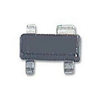
HSMS-2829-TR2G Avago Technologies US Inc., HSMS-2829-TR2G Datasheet - Page 9

HSMS-2829-TR2G
Manufacturer Part Number
HSMS-2829-TR2G
Description
RF DIODE, SCHOTTKY, 1PF 15V SOT-143
Manufacturer
Avago Technologies US Inc.
Datasheet
1.HSMS-2823-BLKG.pdf
(15 pages)
Specifications of HSMS-2829-TR2G
Diode Case Style
SOT-143
No. Of Pins
4
Series Resistance @ If
12ohm
Peak Reflow Compatible (260 C)
Yes
Reel Quantity
1000
Termination Type
SMD
Diode Type
RF Schottky
Voltage - Peak Reverse (max)
15V
Current - Max
1A
Capacitance @ Vr, F
1pF @ 0V, 1MHz
Resistance @ If, F
12 Ohm @ 5mA, 1MHz
Package / Case
SOT-143, SOT-143B, TO-253AA
Rohs Compliant
Yes
Filter Terminals
SMD
Breakdown Voltage Min
15V
Capacitance
1pF
Forward Voltage
340mV
Leaded Process Compatible
Yes
Lead Free Status / RoHS Status
Lead free / RoHS Compliant
Power Dissipation (max)
-
Lead Free Status / RoHS Status
Lead free / RoHS Compliant, Lead free / RoHS Compliant
9
Sampling Applications
The six lead HSMS‑282P can be used in a sampling circuit,
as shown in Figure 25. As was the case with the six lead
HSMS‑282R in the mixer, the open bridge quad is closed
with traces on the circuit board. The quad was not closed
internally so that it could be used in other applications,
such as illustrated in Figure 17.
Figure 25. Sampling Circuit.
Thermal Considerations
The obvious advantage of the SOT‑323 and SOT‑363 over
the SOT‑23 and SOT‑142 is combination of smaller size
and extra leads. However, the copper leadframe in the
SOT‑3x3 has a thermal conductivity four times higher than
the Alloy 42 leadframe of the SOT‑23 and SOT‑143, which
enables the smaller packages to dissipate more power.
The maximum junction temperature for these three fami‑
lies of Schottky diodes is 150°C under all operating con‑
ditions. The following equation applies to the thermal
analysis of diodes:
Tj = (V
where
T
T
θ
V
P
sampling
pulse
sample
a
j
jc
RF
point
f
= junction temperature
I
= diode case temperature
= thermal resistance
f
= RF power dissipated
= DC power dissipated
f
I
f
+ P
RF
HSMS-282P
) θ
jc
+ T
a
sampling circuit
(1)
Note that θ
to the foot of the leads, is the sum of two component re‑
sistances,
Package thermal resistance for the SOT‑3x3 package is ap‑
proximately 100°C/W, and the chip thermal resistance for
the HSMS‑282x family of diodes is approximately 40°C/W.
The designer will have to add in the thermal resistance
from diode case to ambient — a poor choice of circuit
board material or heat sink design can make this number
very high.
Equation (1) would be straightforward to solve but for the
fact that diode forward voltage is a function of tempera‑
ture as well as forward current. The equation for V
where
n = ideality factor
T = temperature in °K
R
and I
I
I
Equation (4) is substituted into equation (3), and equa‑
tions (1) and (3) are solved simultaneously to obtain the
value of junction temperature for given values of diode
case temperature, DC power dissipation and RF power
dissipation.
I
I
s
s
f
f
s
= I
= I
= I
= I
= diode series resistance
θ
0
0
jc
S
S
S
(diode saturation current) is given by
(
(
= θ
e
e
298
298
T
T
pkg
11600 (V
11600 (V
jc
)
)
, the thermal resistance from diode junction
+ θ
n – 4060
n – 4060
2
2
chip
e
e
nT
nT
f
f
– I
– I
f
f
(
(
R
R
1
1
s
s
T
T
)
)
– 1
– 1
–
–
298
298
1
1
)
)
(2)
(3)
(4)
f
is:


