2N5114-E3 Vishay, 2N5114-E3 Datasheet - Page 2
2N5114-E3
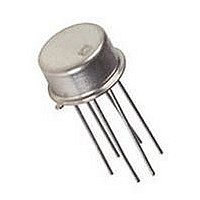
Manufacturer Part Number
2N5114-E3
Description
P CHANNEL JFET, 45V, TO-206AA
Manufacturer
Vishay
Specifications of 2N5114-E3
Breakdown Voltage Vbr
45V
Gate-source Cutoff Voltage Vgs(off) Max
10V
Power Dissipation Pd
500mW
Operating Temperature Range
-55°C To +200°C
No. Of Pins
3
Transistor Polarity
P Channel
Channel Type
P
Configuration
Single
Gate-source Voltage (max)
30V
Drain-gate Voltage (max)
30V
Operating Temperature (min)
-55C
Operating Temperature Classification
Military
Mounting
Through Hole
Pin Count
3
Continuous Drain Current Id
-90mA
Rohs Compliant
Yes
Lead Free Status / RoHS Status
Lead free / RoHS Compliant


2N4338/4339/4340/4341
Vishay Siliconix
www.vishay.com
2
SPECIFICATIONS FOR 2N4338 AND 2N4339 (T
Static
Gate-Source Breakdown Voltage
Gate-Source Cutoff Voltage
Saturation Drain Current
Gate Reverse Current
Gate Reverse Current
Gate Operating Current
Drain Cutoff Current
Gate-Source Forward Voltage
Dynamic
Common-Source
Forward Transconductance
Common-Source
Output Conductance
Drain-Source On-Resistance
Common-Source
Input Capacitance
Common-Source
Reverse Transfer Capacitance
Equivalent Input Noise Voltage
Noise Figure
SPECIFICATIONS FOR 2N4340 AND 2N4341 (T
Static
Gate-Source Breakdown Voltage
Gate-Source Cutoff Voltage
Saturation Drain Current
Gate Reverse Current
Gate Reverse Current
Gate Operating Current
Drain Cutoff Current
Drain Cutoff Current
Gate-Source Forward Voltage
Parameter
Parameter
b
b
b
b
c
c
Symbol
Symbol
V
V
V
V
V
(BR)GSS
V
(BR)GSS
r
I
I
I
I
I
GS(off)
I
D( ff)
D(off)
GS(off)
I
I
I
ds(on)
GS(F)
C
DSS
GSS
GSS
D(off)
C
GSS
GSS
GS(F)
DSS
g
NF
I
g
e
I
G
G
os
iss
rss
fs
n
V
V
V
V
V
V
V
V
DS
DS
DS
DS
DS
DS
DS
DS
V
V
= 15 V V
= 15 V, V
V
V
V
= 15 V V
= 15 V, V
V
V
V
= 10 V, V
V
V
I
I
= 15 V
= 15 V
Test Conditions
= 0 V, V
Test Conditions
I
I
G
DG
DS
f = 1 kHz, R
G
DS
DG
DS
GS
GS
G
G
DS
DS
DS
= −1 mA , V
= −1 mA , V
= 1 mA , V
= 1 mA , V
= 15 V, V
= 15 V, I
= 15 V, I
= 15 V, I
= −30 V, V
= 15 V, I
= −30 V, V
= 15 V, V
= 15 V, V
= 15 V, V
GS
GS
GS
GS
GS
GS
A
A
= 0 V, f = 1 kHz
= 0 V f = 1 MHz
= 0 V, f = 1 MHz
= 0 V, f = 1 kHz
D
D
= 0 V f = 1 kHz
= 0 V, f = 1 kHz
G
D
D
= 25_C UNLESS OTHERWISE NOTED)
GS
= 25_C UNLESS OTHERWISE NOTED)
DS
DS
DS
DS
GS
GS
GS
= 0.1 mA
= 0.1 mA
= 1 MW
DS
DS
= 0.1 mA
= 0.1 mA
= 0 V
= −5 V
= 0 V
= 0 V
= 0 V
= 0 V
= 0 V
= 0 V
= 0 V
= 0 V
V
T
T
V
GS
A
A
GS
= 150_C
= 150_C
= −10 V
= −5 V
Typ
Typ
−57
0.7
1.5
−57
−2
−4
−2
0.7
−2
−4
−2
2
5
6
2
3
a
a
Min
−0.3
Min
−50
0.2
0.6
−50
1.2
−1
2N4338
2N4340
Max
−100
−100
2500
Max
−100
−100
0.6
1.8
50
3.6
−1
50
5
7
3
1
−3
Limits
Limits
S-40990—Rev. F, 24-May-04
Document Number: 70240
Min
−0.6
Min
−50
0.5
0.8
−50
−2
3
2N4339
2N4341
Max
Max
−100
−100
1700
−1.8
−100
−100
1.5
2.4
50
15
−6
70
7
3
1
9
Unit
Unit
√Hz
mA
mS
nV⁄
mA
pA
nA
pA
pA
mS
dB
pF
pF
pA
nA
pA
p
W
V
V
V
V
V
V
Related parts for 2N5114-E3
Image
Part Number
Description
Manufacturer
Datasheet
Request
R

Part Number:
Description:
357-036-542-201 CARDEDGE 36POS DL .156 BLK LOPRO
Manufacturer:
Vishay
Datasheet:
Part Number:
Description:
357-036-542-201 CARDEDGE 36POS DL .156 BLK LOPRO
Manufacturer:
Vishay
Datasheet:
Part Number:
Description:
357-036-542-201 CARDEDGE 36POS DL .156 BLK LOPRO
Manufacturer:
Vishay
Datasheet:
Part Number:
Description:
357-036-542-201 CARDEDGE 36POS DL .156 BLK LOPRO
Manufacturer:
Vishay
Datasheet:
Part Number:
Description:
357-036-542-201 CARDEDGE 36POS DL .156 BLK LOPRO
Manufacturer:
Vishay
Datasheet:
Part Number:
Description:
357-036-542-201 CARDEDGE 36POS DL .156 BLK LOPRO
Manufacturer:
Vishay
Datasheet:
Part Number:
Description:
357-036-542-201 CARDEDGE 36POS DL .156 BLK LOPRO
Manufacturer:
Vishay
Datasheet:
Part Number:
Description:
357-036-542-201 CARDEDGE 36POS DL .156 BLK LOPRO
Manufacturer:
Vishay
Datasheet:
Part Number:
Description:
357-036-542-201 CARDEDGE 36POS DL .156 BLK LOPRO
Manufacturer:
Vishay
Datasheet:
Part Number:
Description:
357-036-542-201 CARDEDGE 36POS DL .156 BLK LOPRO
Manufacturer:
Vishay
Datasheet:
Part Number:
Description:
357-036-542-201 CARDEDGE 36POS DL .156 BLK LOPRO
Manufacturer:
Vishay
Datasheet:
Part Number:
Description:
357-036-542-201 CARDEDGE 36POS DL .156 BLK LOPRO
Manufacturer:
Vishay
Datasheet:
Part Number:
Description:
357-036-542-201 CARDEDGE 36POS DL .156 BLK LOPRO
Manufacturer:
Vishay
Datasheet:
Part Number:
Description:
357-036-542-201 CARDEDGE 36POS DL .156 BLK LOPRO
Manufacturer:
Vishay
Datasheet: