SI3552DV-T1 Vishay, SI3552DV-T1 Datasheet
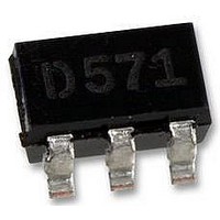
DUAL N/P CHANNEL MOSFET, 30V, TSOP

SI3552DV-T1

Manufacturer Part Number
SI3552DV-T1
Description
DUAL N/P CHANNEL MOSFET, 30V, TSOP
Manufacturer
Vishay
Datasheet

Specifications of SI3552DV-T1

Transistor Polarity
N And P Channel
Continuous Drain Current Id
51A
Drain Source Voltage Vds
30V
On Resistance Rds(on)
360mohm
Rds(on) Test Voltage Vgs
10V
Threshold Voltage Vgs Typ
1V
Lead Free Status / RoHS Status
Contains lead / RoHS non-compliant

Available stocks

Company
Part Number
Manufacturer
Quantity
Price
Part Number:
SI3552DV-T1-E3
Manufacturer:
VIS
Quantity:
20 000
Company:
Part Number:
SI3552DV-T1-E3
Quantity:
70 000
Company:
Part Number:
SI3552DV-T1-E3
Quantity:
901
Part Number:
SI3552DV-T1-GE3
Manufacturer:
VISHAY/威世
Quantity:
20 000
CHARACTERISTICS
DESCRIPTION
SUBCIRCUIT MODEL SCHEMATIC
This document is intended as a SPICE modeling guideline and does not constitute a commercial product data sheet. Designers should refer to the appropriate
data sheet of the same number for guaranteed specification limits.
Document Number: 71514
S-52634Rev. C, 02-Jan-06
• N- and P-Channel Vertical DMOS
• Macro Model (Subcircuit Model)
• Level 3 MOS
The attached spice model describes the typical electrical
characteristics of the n- and p-channel vertical DMOS.
subcircuit
−55 to 125°C temperature ranges under the pulsed 0-V to 5-V gate
drive. The saturated output impedance is best fit at the gate bias
near the threshold voltage.
model
is
extracted
N- and P-Channel 30-V (D-S) MOSFET
and
optimized
over
The
the
SPICE Device Model Si3552DV
• Apply for both Linear and Switching Application
• Accurate over the −55 to 125°C Temperature Range
• Model the Gate Charge, Transient, and Diode Reverse Recovery
A novel gate-to-drain feedback capacitance network is used to model
the gate charge characteristics while avoiding convergence difficulties
of the switched C
to provide a best fit to the measured electrical data and are not
intended as an exact physical interpretation of the device.
Characteristics
gd
model. All model parameter values are optimized
Vishay Siliconix
www.vishay.com
1

Related parts for SI3552DV-T1

SI3552DV-T1 Summary of contents

Page 1

... Document Number: 71514 S-52634Rev. C, 02-Jan-06 SPICE Device Model Si3552DV • Apply for both Linear and Switching Application • Accurate over the −55 to 125°C Temperature Range • Model the Gate Charge, Transient, and Diode Reverse Recovery ...

Page 2

... SPICE Device Model Si3552DV Vishay Siliconix SPECIFICATIONS (T = 25°C UNLESS OTHERWISE NOTED) J Parameter Static Gate Threshold Voltage a On-State Drain Current a Drain-Source On-State Resistance a Forward Transconductance a Diode Forward Voltage b Dynamic Total Gate Charge Gate-Source Charge Gate-Drain Charge Turn-On Delay Time Rise Time ...

Page 3

... COMPARISON OF MODEL WITH MEASURED DATA (T N-Channel MOSFET Document Number: 71514 S-52634Rev. C, 02-Jan-06 SPICE Device Model Si3552DV Vishay Siliconix =25°C UNLESS OTHERWISE NOTED) J www.vishay.com 3 ...

Page 4

... SPICE Device Model Si3552DV Vishay Siliconix P-Channel MOSFET www.vishay.com 4 Document Number: 71514 S-52634Rev. C, 02-Jan-06 ...

Page 5

... Vishay disclaims any and all liability arising out of the use or application of any product described herein or of any information provided herein to the maximum extent permitted by law. The product specifications do not expand or otherwise modify Vishay’ ...

Related keywords