IRF9240 International Rectifier, IRF9240 Datasheet

P CH MOSFET, -200V, 11A, TO-204AA

IRF9240

Manufacturer Part Number
IRF9240
Description
P CH MOSFET, -200V, 11A, TO-204AA
Manufacturer
International Rectifier
Type
Power MOSFETr
Datasheet

Specifications of IRF9240

Transistor Polarity
P Channel
Continuous Drain Current Id
-11A
Drain Source Voltage Vds
-200V
On Resistance Rds(on)
500mohm
Rds(on) Test Voltage Vgs
-10V
Threshold Voltage Vgs Typ
-4V
Number Of Elements
1
Polarity
P
Channel Mode
Enhancement
Drain-source On-res
0.58Ohm
Drain-source On-volt
200V
Gate-source Voltage (max)
±20V
Continuous Drain Current
11A
Power Dissipation
125W
Operating Temp Range
-55C to 150C
Operating Temperature Classification
Military
Mounting
Through Hole
Pin Count
2 +Tab
Package Type
TO-204AA
Lead Free Status / RoHS Status
Contains lead / RoHS non-compliant
Lead Free Status / RoHS Status
Contains lead / RoHS non-compliant

Available stocks

Company
Part Number
Manufacturer
Quantity
Price
Part Number:
IRF9240
Manufacturer:
IR
Quantity:
1 560
Part Number:
IRF9240
Manufacturer:
IR
Quantity:
2
REPETITIVE A V ALANCHE AND dv/dt RATED
HEXFET TRANSISTORS
THRU-HOLE (TO-204AA/AE)
Product Summary
The HEXFET technology is the key to International
Rectifier’s advanced line of power MOSFET transistors.
The efficient geometry and unique processing of this latest
“State of the Art” design achieves: very low on-state resis-
tance combined with high transconductance; superior re-
verse energy and diode recovery dv/dt capability.
The HEXFET transistors also feature all of the well estab-
lished advantages of MOSFETs such as voltage control,
very fast switching, ease of parelleling and temperature
stability of the electrical parameters.
They are well suited for applications such as switching
power supplies, motor controls, inverters, choppers, audio
amplifiers and high energy pulse circuits.
For footnotes refer to the last page
Absolute Maximum Ratings
I D @ V GS = 0V, T C = 25°C
I D @ V GS = 0V, T C = 100°C
www.irf.com
Part Number
IRF9240
P D @ T C = 25°C
T STG
dv/dt
I DM
E AR
E AS
V GS
I AR
T J
BVDSS
-200V
R
0.5
DS(on)
Parameter
Continuous Drain Current
Pulsed Drain Current
Max. Power Dissipation
Linear Derating Factor
Gate-to-Source Voltage
Single Pulse Avalanche Energy
Avalanche Current
Repetitive Avalanche Energy
Peak Diode Recovery dv/dt
Operating Junction
Storage Temperature Range
Lead Temperature
Weight
-11A
I
D
300 (0.063 in. (1.6mm) from case for 10s)
Features:
n
n
n
n
n
Repetitive Avalanche Ratings
Dynamic dv/dt Rating
Hermetically Sealed
Simple Drive Requirements
Ease of Paralleling
11.5(typical)
-55 to 150
200V, P-CHANNEL
12.5
-7.0
-5.0
125
±20
500
-11
-44
-11
1.0
TO-3
IRF9240
PD - 90420
Units
W/°C
V/ns
o
mJ
mJ
W
A
A
V
g
C
01/24/01
1

Related parts for IRF9240

IRF9240 Summary of contents

Page 1

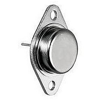
... Weight For footnotes refer to the last page www.irf.com I D -11A Features 300 (0.063 in. (1.6mm) from case for 10s 90420 IRF9240 200V, P-CHANNEL TO-3 Repetitive Avalanche Ratings Dynamic dv/dt Rating Hermetically Sealed Simple Drive Requirements Ease of Paralleling Units -11 -7.0 -44 125 1.0 ±20 ...

Page 2

... IRF9240 Electrical Characteristics Parameter BV DSS Drain-to-Source Breakdown Voltage BV DSS / T J Temperature Coefficient of Breakdown Voltage R DS(on) Static Drain-to-Source On-State Resistance V GS(th) Gate Threshold Voltage g fs Forward Transconductance I DSS Zero Gate Voltage Drain Current I GSS Gate-to-Source Leakage Forward I GSS Gate-to-Source Leakage Reverse Q g Total Gate Charge ...

Page 3

... Fig 1. Typical Output Characteristics Fig 3. Typical Transfer Characteristics www.irf.com Fig 2. Typical Output Characteristics Fig 4. Normalized On-Resistance Vs. Temperature IRF9240 3 ...

Page 4

... IRF9240 Fig 5. Typical Capacitance Vs. Drain-to-Source Voltage Fig 7. Typical Source-Drain Diode Forward Voltage 4 Fig 6. Typical Gate Charge Vs. Gate-to-Source Voltage Fig 8. Maximum Safe Operating Area 13 a& b www.irf.com ...

Page 5

... Fig 9. Maximum Drain Current Vs. Case Temperature Fig 11. Maximum Effective Transient Thermal Impedance, Junction-to-Case www.irf.com D.U. -10V Pulse Width µs Duty Factor Fig 10a. Switching Time Test Circuit t t d(on 10% 90 Fig 10b. Switching Time Waveforms IRF9240 d(off ...

Page 6

... IRF9240 -10V -20V 0 Fig 12a. Unclamped Inductive Test Circuit Fig 12b. Unclamped Inductive Waveforms Q G -10V Charge Fig 13a. Basic Gate Charge Waveform 15V Fig 12c. Maximum Avalanche Energy Fig 13b. Gate Charge Test Circuit Vs. Drain Current Current Regulator Same Type as D.U.T. ...

Page 7

... IR CANADA: 15 Lincoln Court, Brampton, Ontario L6T3Z2, Tel: (905) 453 2200 IR GERMANY: Saalburgstrasse 157, 61350 Bad Homburg Tel (0) 6172 96590 IR ITALY: Via Liguria 49, 10071 Borgaro, Torino Tel 011 451 0111 Data and specifications subject to change without notice. 1/01 -11A, di/dt -150A/ s, 150°C 300 s; Duty Cycle 2% IRF9240 7 ...

Related keywords