MTM981400BBF Panasonic, MTM981400BBF Datasheet
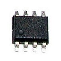
MOSFET, P-CH, 40V, 7A, S08

MTM981400BBF

Manufacturer Part Number
MTM981400BBF
Description
MOSFET, P-CH, 40V, 7A, S08
Manufacturer
Panasonic
Datasheet

Specifications of MTM981400BBF

Transistor Polarity
P Channel
Drain Source Voltage Vds
-40V
Transistor Case Style
SOIC
No. Of Pins
8
Svhc
No SVHC (18-Jun-2010)
Current Id Max
-7A
Power Dissipation Pd
2W
Lead Free Status / RoHS Status
Lead free / RoHS Compliant
Small-Signal Short-Circuit Imput Capacitance
Small-Signal Short-Circuit Output Capacitance
Small-Signal Reverse Transfer Capacitance
Type
Application
Structure
Outline
Absolute Maximum
Ratings
Drain-Source Voltage
Drain-Source Cutoff Current
Gate-Source Cutoff Current
Gate Threshold Voltage
Drain Resistance (ON)
Forward Transfer Admittance
Turn-on Delay Time
Rise Time
Turn-off Delay Time
Fall Time
Product Specification
Type Number : M T M 9 8 1 4 0 0 B B F
Note:
Established
2008.01.31
Measuring methods are based on JAPANESE INDUSTRIAL STANDARD JIS C 7030 Measuring
methods for transistors.
*1 Packing
*2 Measuring on ceramic board at 50×50×1.0mm.
*3
*4 See test circuit
Embossed type (thermo-compressioon sealing)
Pulse test
Item
Revised
Silicon Field Effect Transistors
Switching
P-Channel MOS Type
SO8-F1-B
VDSS
-40
(V)
*3,4
*3,4
*3,4
*3,4
*3
*3
*3
RDS(ON)
RDS(ON) ID = -3.5A, VGS = -4.5V
Electrical characteristics (Ta = 25 °C ±3 °C)
VGSS
Symbol
±20
VDSS
td(off)
td(on)
(V)
IGSS
IDSS
Coss
Crss
|Yfs|
Ciss
Vth
tr
tf
*1
VDD = -25 V, VGS = 0 to -10 V, ID = -3.5 A
VDD = -25 V, VGS = -10 to 0 V, ID = -3.5 A
VDS = -10 V, VGS = 0 V, f = 1MHz
VDS = -10V, VGS = 0V, f = 1MHz
VDS = -10 V, VGS = 0 V, f = 1 MHz
ID = -1 mA, VGS = 0 V
VDS = -40 V, VGS = 0 V
VGS = ±16 V, VDS = 0 V
ID = -1.0 mA, VDS = -10.0 V
ID = -7 A, VGS = -10 V
ID = -7 A, VDS = -10 V
(A)
ID
-7
Measuring condition
Panasonic Semiconductor Discrete Devices Co., Ltd.
IDp
-28
(A)
Prepared
PD
S.Miyata
(W)
2
by
*2
1.Source
2.Source
3.Source
4.Gate
5.Drain
6.Drain
7.Drain
8.Drain
(°C)
Tch
150
M.Fujisawa
Checked
Internally connected circuit
by
-55 to +150
Marking
Tstg
min.
(°C)
-1.0
-40
10
1
1
1
1
2
2
2
2
3
3
3
3
4
4
4
4
H.Shidooka
Applied
Limit
2700
typ.
190
175
230
19
28
18
15
70
by
Sheet No. 1 / 2
max.
-2.5
±10
-10
25
45
8
8
8
8
7
7
7
7
6
6
6
6
5
5
5
5
Established
BA
by
Unit
m
m
pF
pF
pF
ns
ns
ns
ns
V
V
S
A
A

Related parts for MTM981400BBF

MTM981400BBF Summary of contents

Page 1

... Coss VDS = -10V, VGS = 0V 1MHz Crss VDS = -10 V, VGS = MHz td(on) VDD = -25 V, VGS = VDD = -25 V, VGS = -3.5 A td(off) VDD = -25 V, VGS = - -3 VDD = -25 V, VGS = - -3.5 A Panasonic Semiconductor Discrete Devices Co., Ltd. Checked Applied S.Miyata M.Fujisawa H.Shidooka Marking *2 PD Tch ...

Page 2

... Product Specification Type Number : Test circuit Vin D.C. -10V Vin Vin Vout 2008.01.31 Established Revised *1 VDD = - td(on) tr td(off) Panasonic Semiconductor Discrete Devices Co., Ltd. Sheet No -3 7.1 Vout ...

Page 3

... Regulations No. : SC3S1512 PACKAGE STANDARDS Package Code Established by H.Shidooka : 2009-01-23 SO8-F1-B Semiconductor Company Panasonic Corporation Applied by Checked by H.Yoshida M.Okajima Total Pages Page 3 1 Prepared by M.Kametaka ...

Page 4

... Outline Drawing : 2009-01-23 PACKAGE STANDARDS SO8-F1-B Body Material Lead Material Lead Finish Method : SnBi Plating Semiconductor Company, Panasonic Corporation Total Pages Page 3 2 Unit: Free : Epoxy Resin : Cu Alloy ...

Page 5

... Mark Drawing The First Pin Position : 2009-01-23 PACKAGE STANDARDS SO8-F1-B Product Name (Shortened Name) Date Code Semiconductor Company, Panasonic Corporation Total Pages Page 3 3 ...

Related keywords