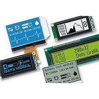
BTHQ128064AVD-COG-SRE BATRON, BTHQ128064AVD-COG-SRE Datasheet - Page 10

BTHQ128064AVD-COG-SRE
Manufacturer Part Number
BTHQ128064AVD-COG-SRE
Description
LCD MODULE, 128X64, GRAPHIC
Manufacturer
BATRON
Datasheet
1.BTHQ128064AVD-COG-SRE.pdf
(16 pages)
Specifications of BTHQ128064AVD-COG-SRE
Lcd Display Type
STN
Pixel Size (h X W)
0.349mm X 0.418mm
Interface Type
Serial
Viewing Area (h X W)
31mm X 50.6mm
Supply Voltage
3.3V
External Depth
1.8mm
External Length /
RoHS Compliant
Display Mode
Reflective
Svhc
No SVHC (15-Dec-2010)
Rohs Compliant
Yes
Pixel Pitch (h X W)
0.364mm X 0.433mm
DATA MODUL AG Landsberger Str. 322 80687 München Tel.: 089/ 56017-0 Fax 089/ 56017-119
Pin No.
16
17
18
19
20
21
22
23
24
25
26
27
28
R/W(WR) When connected to an 8080 MPU, this is active LOW.
Symbol
E(RD)
RES
D/C
CS1
D7
D6
D5
D4
D3
D2
D1
D0
This is an 8-bit bi-directional data bus that connects to an 8-bit standard MPU
data bus.
When the serial interface is selected (P/S = LOW), then D7 serves as the serial
data input terminal (SI) and D6 serves as the serial clock input terminal (SCL).
At this time, D0 to D5 are set to high impedance.
When the chip select is inactive, D0 to D7 are set to high impedance.
When connected to an 8080 MPU, this is active LOW.
This pin is connected to the RD signal of the 8080 MPU, and the S1D15605
series data bus is in an output status when this signal is LOW.
When connected to a 6800 Series MPU, this is active HIGH.
This is the 6800 Series MPU enable clock input terminal.
This terminal connects to the 8080 MPU WR signal. The signals on the data
bus are latched at the rising edge of the WR signal.
When connected to an 6800 Series MPU:
This is the read/write control signal input terminal.
When R/W = HIGH: Read.
When R/W = LOW: Write.
This is connect to the least significant bit of the normal MPU address bus, and
it determines whether the data bits are data or a command.
D/C(A0)=“High”: Indicates that D0 to D7 are display data.
D/C(A0)=“Low”: Indicates that D0 to D7 are control data.
This is the chip select signal for first chip.
When CS1=LOW and CS2=HIGH, then the chip select becomes active and the
data/commands I/O is enabled.
When RES is set to LOW, the settings are initialized.
The reset operation is performed by the RES signal level.
Table 2(b): Pin Assignment
Description
VL-FS-COG-BTD12864-01 REV. A
(BTHQ 128064AVD-SRE-06-COG)
JULY/2003
PAGE 10 OF 16
www.data-modul.de


