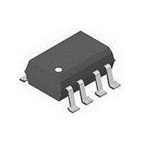
IL300-DEFG-X007 Vishay, IL300-DEFG-X007 Datasheet - Page 10

IL300-DEFG-X007
Manufacturer Part Number
IL300-DEFG-X007
Description
OPTOCOUPLER, PHOTODIODE, 5300VRMS
Manufacturer
Vishay
Datasheet
1.IL300-DEFG-X007.pdf
(11 pages)
Specifications of IL300-DEFG-X007
No. Of Channels
1
Optocoupler Output Type
Photodiode
Input Current
10mA
Output Voltage
50V
Opto Case Style
SMD
No. Of Pins
8
Peak Reflow Compatible (260 C)
No
Isolation Voltage
5.3kV
Current Transfer Ratio
0.5 % to 1.1 %
Forward Current
10 mA
Maximum Fall Time
1.75 us
Maximum Rise Time
1.75 us
Output Device
PIN Photodiode
Output Type
DC
Configuration
1 Channel
Input Type
AC/DC
Maximum Forward Diode Voltage
1.5 V
Maximum Reverse Diode Voltage
5 V
Maximum Input Diode Current
60 mA
Maximum Power Dissipation
210 mW
Maximum Operating Temperature
+ 100 C
Minimum Operating Temperature
- 55 C
Package / Case
SMD-8
Number Of Elements
1
Reverse Breakdown Voltage
5V
Forward Voltage
1.5V
Collector-emitter Voltage
Not RequiredV
Package Type
PDIP SMD
Collector Current (dc) (max)
Not RequiredA
Power Dissipation
210mW
Collector-emitter Saturation Voltage
Not RequiredV
Pin Count
8
Mounting
Surface Mount
Operating Temp Range
-55C to 100C
Operating Temperature Classification
Industrial
Lead Free Status / RoHS Status
Lead free / RoHS Compliant
Lead Free Status / RoHS Status
Lead free / RoHS Compliant, Lead free / RoHS Compliant
Available stocks
Company
Part Number
Manufacturer
Quantity
Price
IL300
Vishay Semiconductors
These amplifiers provide either an inverting or non-inverting
transfer gain based upon the type of input and output
amplifier. Table 2 shows the various configurations along
with the specific transfer gain equations. The offset column
refers to the calculation of the output offset or V
necessary to provide a zero voltage output for a zero voltage
input. The non-inverting input amplifier requires the use of a
bipolar supply, while the inverting input stage can be
implemented with single supply operational amplifiers that
PACKAGE DIMENSIONS in millimeters
PACKAGE MARKING (this is an example of the IL300-E-X001)
www.vishay.com
10
i178010
0.406
0.508
Option 6
0.527
0.889
10.36
10.16
10.92
9.96
7.8
7.4
7.112
8.382
0.35
0.25
For technical questions, contact:
1.016
1.270
3.302
3.810
Linear Optocoupler, High Gain
21764-41
Stability, Wide Bandwidth
0.203
0.305
0.508 ref.
0.7
9.652
10.16
Pin one ID
X001
V YWW H 68
IL300-E
ref2
Option 7
10.3 max.
7.62 typ.
8.4 min.
1
2
3
4
8 min.
3°
9
7.62 typ.
optocoupleranswers@vishay.com
permit operation close to ground.
For best results, place a buffer transistor between the LED
and output of the operational amplifier when a CMOS
opamp is used or the LED I
beyond
magnitude of the closed loop gain of the input and output
amplifiers. Best bandwidths result when the amplifier gain is
designed for unity.
10°
8
7
6
5
6.096
6.604
4.6
4.1
0.254 ref.
2.794
3.302
4°
15 mA. Finally the bandwidth is influenced by the
0.102
0.249
0.254 ref.
ISO method A
1.270
2.540
Option 9
Fq
7.62 ref.
10.03
9.53
8 min.
0.51
1.02
drive is targeted to operate
Document Number: 83622
Rev. 1.6, 10-Nov-10
15° max.
0.25 typ.
18450


