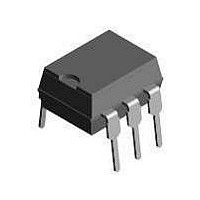
CNY17F-3X001 Vishay, CNY17F-3X001 Datasheet - Page 16

CNY17F-3X001
Manufacturer Part Number
CNY17F-3X001
Description
Optocoupler
Manufacturer
Vishay
Specifications of CNY17F-3X001
Leaded Process Compatible
Yes
Forward Current
60 mA
Maximum Input Diode Current
60 mA
Maximum Reverse Diode Voltage
6 V
Output Device
Transistor
Output Type
DC
Configuration
1
Input Type
DC
Maximum Collector Emitter Voltage
70 V
Maximum Collector Emitter Saturation Voltage
400 mV
Isolation Voltage
5300 Vrms
Current Transfer Ratio
200 %
Maximum Forward Diode Voltage
1.65 V
Maximum Collector Current
100 mA
Maximum Power Dissipation
150 mW
Maximum Operating Temperature
+ 100 C
Minimum Operating Temperature
- 55 C
Package / Case
PDIP-6
No. Of Channels
1
Optocoupler Output Type
Phototransistor
Input Current
60mA
Output Voltage
70V
Opto Case Style
DIP
No. Of Pins
6
Approval Bodies
UL, IEC65, IEC950, BS6301,
Rohs Compliant
Yes
Lead Free Status / RoHS Status
Lead free / RoHS Compliant
Lead Free Status / RoHS Status
Lead free / RoHS Compliant, Lead free / RoHS Compliant
Available stocks
Company
Part Number
Manufacturer
Quantity
Price
Option Information
Vishay Semiconductors
OPTION 8
LEAD
OPTOCOUPLERS
These optocouplers are suitable for surface mounting.
Dimensions deviating from the standard type are:
Creepage distance > 8.0 mm
Clearance distance > 8.0 mm
This version additionally complies with the following
standards:
• IEC 60950 DIN VDE 0805/05 90 (system 2 and 3 only)
During the soldering process, the package should not be
wetted with tin-lead solder to prevent the impairment of the
isolation features. Apart from iron soldering, only reflow
soldering methods (vapor phase, infrared and hot gas) are
permissible.
Permissible soldering conditionsfor SMD bending options:
please see reflow soldering profile
The soldering process may be repeated two times at the
most. Attention must be paid to the cooling down of the
device to 25 °C between the soldering processes
Clearance and creepage distances must be considered for
the solder pad design.
Clearance-creepage distance = 8.0 min.
See standard version for pin configuration.
OPTION 9
LEAD BENDS FOR SURFACE MOUNT
OPTOCOUPLERS
During the soldering process, the package should not be
wetted with tin-lead solder to prevent the impairment of the
isolation features. Apart from iron soldering, only reflow
soldering methods (vapor phase, infrared and hot gas) are
www.vishay.com
6
0.020 (0.50)
0.000 (0.00)
0.000 (0.00)
0.020 (0.50)
17932
Reinforced insulation up to an operating voltage of
400 V
RMS
BENDS
or DC
0.47 2 (12.00)
0.47 2 (12.00)
0.365 (9.27)
0.365 (9.27)
0.300 (7.62)
0.300 (7.62)
min.
min.
typ.
max.
typ.
max.
FOR
0.150 (3.81)
0.130 (3.30)
0.150 (3.81)
0.130 (3.30)
SURFACE
For technical questions, contact: optocoupler.answers@vishay.com
0.015 (0.38)
0.020
(0.5)
typ.
DIP 6
DIP 4
0.020(0.5)
0.05 (1.27)
0.040(1.02)
MOUNT
typ.
0.016 (0.4)
0.031 (0.79)
Option Information
typ.
permissible.
Permissible soldering conditionsfor SMD bending options:
please see reflow soldering profile
The soldering process may be repeated two times at the
most. Attention must be paid to the cooling down of the
device to 25 °C between the soldering processes.
MARKINGS
The following table defines the option information that is
marked on the product.
0.0098 (0.249)
0.0040 (0.102)
17933
0.015 (0.38)
OPTION TYPE
X001, X001T
X007, X007T
X008, X008T
X009, X009T
X017, X017T
X018, X018T
X019, X019T
typ.
X006
X016
DIP4/ 8/16
0.050 (1.27)
0.040 (1.02)
0.020 (0.51)
0.395 (10.03 )
0.375 (9.53)
0.300 (7.62)
typ.
0.016 (0.4)typ.
0.031(0.79)
ref.
0.020
(0.5)
typ.
Document Number: 83713
DIP 6
MARKING
No mark
No Mark
Rev. 1.7, 11-Sep-07
X001
X007
X008
X001
X017
X018
X001
0.012 (0.30) typ.
15° m ax.
0.020 (0.5)
0.040 (1.02)


