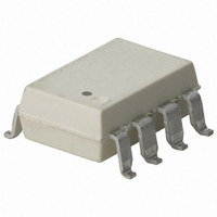
HCPL-7510-300 Avago Technologies US Inc., HCPL-7510-300 Datasheet - Page 8

HCPL-7510-300
Manufacturer Part Number
HCPL-7510-300
Description
Optocoupler
Manufacturer
Avago Technologies US Inc.
Datasheet
1.HCPL-7510-000E.pdf
(17 pages)
Specifications of HCPL-7510-300
No. Of Channels
1
Isolation Voltage
3.75kV
Optocoupler Output Type
Analog
Input Current
16mA
Output Voltage
6V
Opto Case Style
SMD
No. Of Pins
8
Peak Reflow Compatible (260 C)
No
Bandwidth
100kHz
Amplifier Type
Isolation
Number Of Circuits
1
-3db Bandwidth
100kHz
Current - Input Bias
600nA
Voltage - Input Offset
600µV
Current - Supply
11.7mA
Current - Output / Channel
16mA
Voltage - Supply, Single/dual (±)
4.5 V ~ 5.5 V
Operating Temperature
-40°C ~ 85°C
Mounting Type
Surface Mount
Package / Case
8-SMD Gull Wing
Lead Free Status / RoHS Status
Contains lead / RoHS non-compliant
Output Type
-
Slew Rate
-
Gain Bandwidth Product
-
Lead Free Status / RoHS Status
Contains lead / RoHS non-compliant, Contains lead / RoHS non-compliant
Other names
516-1137-5
Available stocks
Company
Part Number
Manufacturer
Quantity
Price
Company:
Part Number:
HCPL-7510-300
Manufacturer:
AVAGO
Quantity:
7 500
Company:
Part Number:
HCPL-7510-300E
Manufacturer:
AVAGO
Quantity:
7 500
Part Number:
HCPL-7510-300E
Manufacturer:
AVAGO/安华高
Quantity:
20 000
Switching Specifications (AC)
Over recommended operating conditions unless otherwise specified.
Parameter
V
V
V
V
V
V
V
Common Mode Transient
Immunity
Package Characteristics
Parameter
Input-Output Momentary
Withstand Voltage
Input-Output Resistance
Input-Output Capacitance
Notes:
General Note: Typical values were taken from a sample of nominal units operating at nominal conditions (V
ture = 25°C) unless otherwise stated. Nominal plots shown from Figure 1 to 11 represented the drift of these nominal units from their nominal
operating conditions.
1. Input Offset Voltage is defined as the DC Input Voltage required to obtain an output voltage of V
2. Gain is defined as the slope of the best-fit line of the output voltage vs. the differential input voltage (V
3. Nonlinearity is defined as half of the peak-to-peak output deviation from the best-fit gain line, expressed as a percentage of the full-scale output
4. NL
5. NL
6. In accordance with UL1577, each optocoupler is proof tested by applying an insulation test voltage
7. CMRR is defined as the ratio of the differential signal gain (signal applied differentially between pins 2 and 3) to the common-mode gain (input
8
IN
IN
IN
OUT
OUT
OUT
OUT
Gain is derived from V
voltage range.
detection current limit, I
IEC/EN/DIN EN 60747-5-2 Insulation Characteristic Table, if applicable.
pins tied together and the signal applied to both inputs at the same time), expressed in dB.
to V
to V
to V
200
100
Rise Time (10 – 90%)
Fall Time (10 – 90%)
Bandwidth (-3 dB)
Noise
OUT
OUT
OUT
is the nonlinearity specified over an input voltage range of ±200 mV.
is the nonlinearity specified over an input voltage range of ±100 mV.
Signal Delay (50 – 10%)
Signal Delay (50 – 50%)
Signal Delay (50 – 90%)
REF
/512 mV; e.g. V
I-O
≤
5 µA). This test is performed before the 100% production test for the partial discharge (method b) shown in
Symbol
V
R
C
ISO
I-O
I-O
REF
Symbol
t
t
t
t
t
BW
N
CMTI
= 5.0, gain will be 9.77 V/V.
PD10
PD50
PD90
R
F
OUT
Min.
3750
Min.
50
10
Typ.
>10
1.4
Typ.
2.2
3.4
5.2
3.0
3.2
100
31.5
15
9
Max.
4
5
9.9
7
7
Max.
Units
µs
µs
µs
µs
µs
kHz
mVrms
kV/µs
Units
V
Ω
pF
rms
Test Conditions
V
V
V
T
A
IN+
IN+
IN+
= 25°C, V
REF
Test Conditions
T
V
Freq = 1 MHz
= 0 mV to 200 mV step
= 200 mV
= 0 V
A
I-O
/2.
= 25°C, RH < 50%
= 500 V
IN+
DD1
≥
- V
CM
= V
4500 Vrms for 1 second (leakage
IN-
pk-pk
= 1000 V
) over the specified input range.
DD2
= 5 V, V
REF
= 4.0 V, Tempera-
Fig.
Fig. Note
13
14
15
Note
6


