VLMS30J1K2-GS18 Vishay, VLMS30J1K2-GS18 Datasheet
VLMS30J1K2-GS18
Specifications of VLMS30J1K2-GS18


Related parts for VLMS30J1K2-GS18

VLMS30J1K2-GS18 Summary of contents
Page 1
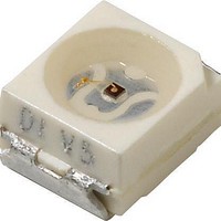
... Package: SMD PLCC-2 • Product series: low current • Angle of half intensity: ± 60° PARTS TABLE PART VLMS3000-GS08 VLMS3000-GS18 VLMS30J1K2-GS08 VLMS30J1K2-GS18 VLMS30K1L2-GS08 VLMS30K1L2-GS18 Document Number 81322 Rev. 1.3, 30-Sep-10 VLMO30.., VLMS30.., VLMY30.. Low Current SMD LED FEATURES • SMD LED with exceptional brightness • ...
Page 2
... VLMO30.., VLMS30.., VLMY30.. Vishay Semiconductors PARTS TABLE PART VLMS30J1L2-GS08 VLMS30J1L2-GS18 VLMS30J2K2-GS08 VLMS30J2K2-GS18 VLMS30K2L2-GS08 VLMO3000-GS08 VLMO3000-GS18 VLMO30K1L2-GS08 VLMO30K1L2-GS18 VLMO30L1M2-GS08 VLMO30L1M2-GS18 VLMO30K1M2-GS08 VLMO30K1M2-GS18 VLMY3000-GS08 VLMY3000-GS18 VLMY3001GS08 VLMY3001-GS18 VLMY30J2L1-GS08 VLMY30J2L1-GS18 VLMY30K2M1-GS08 VLMY30K2M1-GS18 VLMY30J2M1-GS08 VLMY30J2M1-GS18 ABSOLUTE MAXIMUM RATINGS (T PARAMETER 1) Reverse voltage DC forward current Surge forward current ...
Page 3
... Peak wavelength Angle of half intensity Forward voltage Reverse voltage Note: 1) ≤ 1.6 In one packing unit I /I Vmax. Vmin. Document Number 81322 Rev. 1.3, 30-Sep-10 VLMO30.., VLMS30.., VLMY30 °C, unless otherwise specified) amb TEST CONDITION PART VLMS3000 VLMS3000 VLMS30J1K2 VLMS30K1L2 VLMS30J1L2 VLMS30J2K2 VLMS30K2L2 ...
Page 4
... Note: 22.4 Wavelengths are tested at a current pulse duration and an accuracy of ± 1 nm. 28.0 CROSSING TABLE VLMO30K1L2 VLMO30K1M2 VLMO30L1M2 VLMS30J1K2 VLMS30K1L2 VLMY30J2M1 VLMY30K2M1 = 25 °C, unless otherwise specified) amb 1000 80 100 17557 For technical support, please contact: LED@vishay.com YELLOW ORANGE DOM ...
Page 5
... Figure 6. Rel. Luminous Intensity vs. Ambient Temperature red 660 700 18252 Figure 7. Forward Voltage vs. Ambient Temperature 2.5 3 For technical support, please contact: LED@vishay.com Vishay Semiconductors 2.50 yellow 2.25 2.00 orange 1.75 red 1.50 1.25 1.00 0.75 0.50 0.25 ...
Page 6
... VLMO30.., VLMS30.., VLMY30.. Vishay Semiconductors PACKAGE DIMENSIONS in millimeters 3.5 ± 0.2 Pin identification C Ø 2.4 + 0.15 3 Drawing-No.: 6.541-5067.01-4 Issue: 5; 04.11.08 20541 www.vishay.com 6 A 1.6 (1.9) For technical support, please contact: LED@vishay.com technical drawings according to DIN specifications Mounting Pad Layout 1.2 area covered with ...
Page 7
... METHOD OF TAPING/POLARITY AND TAPE AND REEL SMD LED (VLM.3 - SERIES) Vishay’s LEDs in SMD packages are available in an antistatic 8 mm blister tape (in accordance with DIN IEC 40 (CO) 564) for automatic component insertion. The blister tape is a plastic strip with impressed component cavities, covered by a top tape. ...
Page 8
... Time (s) 19885 Figure 11. Vishay Lead (Pb)-free Reflow Soldering Profile (acc. to J-STD-020) TTW Soldering (acc. to CECC00802) 300 5 s lead temperature 250 235 °C second wave full line: typical to 260 °C ...
Page 9
... Vishay product could result in personal injury or death. Customers using or selling Vishay products not expressly indicated for use in such applications their own risk and agree to fully indemnify and hold Vishay and its distributors harmless from and against any and all claims, liabilities, expenses and damages arising or resulting in connection with such use or sale, including attorneys fees, even if such claim alleges that Vishay or its distributor was negligent regarding the design or manufacture of the part ...