L5104 VERMASON, L5104 Datasheet - Page 3
L5104
Manufacturer Part Number
L5104
Description
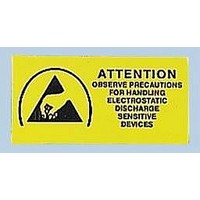
LABEL, WARNING, 12.5MMX12.5MM, 1000PCS
Manufacturer
VERMASON
Datasheet
1.L5104.pdf
(12 pages)
Specifications of L5104
Label Type
Warning
Label Size
12.5 X 12.5mm
Label Material
Paper
Background Color
Yellow
Legend
Attention Observe Precautions For Handling Electrostatic Discharge Sensitive Devices Symbol
Lead Free Status / RoHS Status
Lead free / RoHS Compliant


PrintDate=1997/09/29 PrintTime=12:36:21 18016 ds011061 Rev. No. 1 cmserv
V
V
I
I
GBW
SR
PBW
t
e
i
OSC
S
Symbol
n
s
These limits apply for supply voltage =
face are for T
O
O
m
n
DC Electrical Characteristics
AC Electrical Characteristics
These limits apply for supply voltage =
standard typeface are for T
Note 1: Absolute maximum ratings indicate limits beyond which damage to the component may occur. Electrical specifications do not apply when operating the de-
vice beyond its rated operating conditions.
Note 2: The ESD protection circuitry between the inputs will begin to conduct when the differential input voltage reaches 8V.
Note 3: a) In addition, the voltage between the V
3V below the negative supply pin voltage, a substrate diode begins to conduct. Current
through this pin must then be kept less than 20 mA to limit damage from self-heating.
Note 4: Although the output current is internally limited, continuous short-circuit operation at elevated ambient temperature can result in exceeding the maximum al-
lowed junction temperature of 150˚C.
Note 5: This value is the average voltage that the weakest pin combinations can withstand and still conform to the datasheet limits. The test circuit used consists
of the human body model, 100 pF in series with 1500 .
Note 6: The typical thermal resistance, junction-to-ambient, of the molded plastic DIP (N package) is 105˚C/W. For the molded plastic SO (M package), use 155˚C/W.
All numbers apply for packages soldered directly into a printed circuit board.
Note 7: Typical values are for T
Note 8: Limits are guaranteed, by testing or correlation.
Symbol
Gain-Bandwidth Product
Slew Rate
Power Bandwidth
Settling Time
Phase Margin
Differential Gain
Differential Phase
Input Noise Voltage
Input Noise Current
A
Output Voltage
Swing
Output Voltage Swing
Output Short
Circuit Current
Supply Current
= T
Parameter
J
= 25˚C; limits in boldface type apply over the Operating Temperature Range.
Parameter
J
= 25˚C, and represent the most likely parametric norm.
A
= T
J
= 25˚C; limits in boldface type apply over the Operating Temperature Range .
+
±
±
Supply =
Supply = +5V and
R
Sourcing
Sinking
pin and either input pin must not exceed 36V.
15V, V
f = 20 MHz
A
V
10V step, to 0.1%
A
A
NTSC, A
NTSC, A
f = 10 kHz
f = 10 kHz
15V, V
L
V
OUT
V
V
= 2 k
= +2 (Note 11)
= −1, R
= +2
Conditions
= 20 V
CM
CM
Supply =
Supply =
(Continued)
Conditions
V
V
±
= 0V, and R
(Note 10)
= 0V, R
15V, R
= +2
= +2
L
PP
= 2 k
±
±
L
L
5V
5V
= 2 k
3
100 k , and C
L
Typical
(Note
<
<
100 k , unless otherwise specified. Limits in standard type-
100
300
200
100
4.5
1.2
70
45
10
7)
0.1
0.1
+14.2
(Note 7)
Typical
−13.4
4.2
1.3
5.0
65
65
(Note 8)
LM6162
L
Limit
200
180
80
55
5 pF, unless otherwise specified. Limits in
LM6162
(Note 8)
Proof
+13.5
+13.3
−13.0
−12.7
Limit
3.5
3.3
1.7
2.0
6.5
6.8
30
20
30
20
(Note 8)
LM6262
Limit
200
180
80
65
(Note 8)
LM6262
Limit
+13.5
+13.3
−13.0
−12.8
3.5
3.3
1.7
1.9
6.5
6.7
30
25
30
25
(Note 8)
LM6362
Limit
200
180
75
65
(Note 8)
LM6362
+13.4
−12.9
−12.8
Limit
13.3
3.4
3.3
1.8
1.9
6.8
6.9
30
25
30
25
www.national.com
nV/ Hz
pA/ Hz
Units
MHz
MHz
V/µs
V/µs
MHz
min
min
deg
deg
ns
Units
%
max
max
max
min
min
min
min
mA
mA
mA
V
V
V
V
3
Related parts for L5104
Image
Part Number
Description
Manufacturer
Datasheet
Request
R

Part Number:
Description:
T1 3/4 Front Mount LED Indicator
Manufacturer:
Wilbrecht Electronics, Inc.