T7G-434.075 QUASAR, T7G-434.075 Datasheet - Page 5
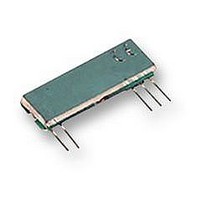
T7G-434.075
Manufacturer Part Number
T7G-434.075
Description
TRANSMITTER, NARROW BAND, 434.075
Manufacturer
QUASAR
Datasheet
1.R7G-434.075.pdf
(7 pages)
Specifications of T7G-434.075
Svhc
No SVHC (18-Jun-2010)
Current Rating
25mA
Data Rate Max
20Kbps
External Depth
10mm
External Length / Height
3.5mm
External Width
31mm
Frequency
434.075MHz
Operating Temperature Max
70°C


Transmitter Connection Diagram
Figure 1: Narrow Band T7 / T7G Transmitters
Pin Description:
RF GND (pin 1)
RF ground pin, internally connected to pin 4 (0v).
This pin should ideally be connected to the
nearest ground plane ( e.g coax braid, main PCB
ground plane etc. ).
RF OUT (pin 2)
50 Ohm RF antenna output. To achieve best
results, the antenna impedance must match that
of the module.
Vcc (pin 3)
+Ve supply pin. The module will generate RF
when Vcc is present.
GND (pin 4)
Supply and data ground connection, connected to
pin 1.
Data IN (pin 5)
This input has an impedance of 47K Ohms and
should ideally be driven by a CMOS logic drive or
compatible. The drive circuitry should be supplied
with the same supply voltage as the TX module.
DS307-7 Oct 05
T7
1
2
3
FM 433MHz Narrow Band
4
©2004 REG No 277 4001, England.
5
Receiver Connection Diagram
Figure 2: Narrow Band R7 / R7G Receivers
Pin Description:
RF IN ( pin 1)
50 Ohm RF input from antenna, connect using
shortest possible route. This input is isolated from
the internal circuit using the air gap of the front
end SAW RF filter.
RF GND (pin 2)
RF Ground connection, preferably connected to a
solid ground plane.
RSSI / Carrier Detect (pin 3)
The Received Signal Strength Indicator provides a
DC output voltage proportional to the RF input
signal. The amplitude of the RSSI voltage
increases with increasing RF signal strength. A
simple transistor interface can yield a carrier
detect logic output.
GND (pin 4)
Connect to power supply ground.
VCC (pin 5)
+Ve supply pin. Operation from a 5V supply able
to source 10mA at less than 10mV p-p ripple.
AF (pin 6)
Audio frequency output ( max 40microA source )
DATA OUT (pin 7)
CMOS compatible output. This may be used to
drive external decoders. To reduce any noise on
this output add a 56pF cap from this pin to GND.
R7
1 2
Page 5
3 4 5 6 7
T7G / R7G
T7 / R7
Related parts for T7G-434.075
Image
Part Number
Description
Manufacturer
Datasheet
Request
R

Part Number:
Description:
TRANSMITTER, NARROW BAND, 434.525
Manufacturer:
QUASAR
Datasheet:

Part Number:
Description:
REMOTE CONTROL SYSTEM, 1CH, 60M
Manufacturer:
QUASAR
Datasheet:

Part Number:
Description:
MODULE, TRANSMITTER, AM, 433MHZ
Manufacturer:
QUASAR
Datasheet: