AD9913/PCBZ Analog Devices Inc, AD9913/PCBZ Datasheet - Page 25
AD9913/PCBZ
Manufacturer Part Number
AD9913/PCBZ
Description
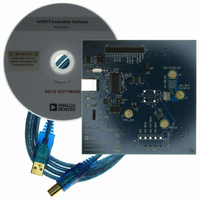
Eval Board
Manufacturer
Analog Devices Inc
Series
AgileRF™r
Datasheet
1.AD9913BCPZ.pdf
(32 pages)
Specifications of AD9913/PCBZ
Silicon Manufacturer
Analog Devices
Application Sub Type
Direct Digital Synthesizer
Kit Application Type
Clock & Timing
Silicon Core Number
AD9913
Kit Contents
Board
Tool / Board Applications
D/A Converter
Main Purpose
Timing, Direct Digital Synthesis (DDS)
Embedded
No
Utilized Ic / Part
AD9913
Primary Attributes
10-Bit DAC, 32-Bit Tuning Word Width
Secondary Attributes
250MHz, Graphical User Interface
Lead Free Status / RoHS Status
Lead free / RoHS Compliant


REGISTER UPDATE (I/O UPDATE)
Functionality of the I/O UPDATE and SYNC_CLK
Data from a write sequence is stored in a buffer register (data
inactive). An active register exists for every buffer register. The
I/O update signal and SYNC_CLK are used to transfer the
contents from the buffer register into the active register.
I/O_UPDATE initiates the start of a buffer transfer. It can be
sent synchronously or asynchronously relative to the SYNC_CLK.
If the setup time between the two signals is met, then constant
latency (pipeline) to the DAC output exists. For example, if
constant propagation delay of phase offset changes via the SPI
BUFFER REGISTER
ACTIVE REGISTER
I/O_UPDATE
SYNC_CLK
DATA IN
DATA IN
THE DEVICE REGISTERS AN I/O UPDATE AT POINT A. THE DATA IS TRANSFERRED FROM
THE ASYNCHRONOUSLY LOADED I/O BUFFERS AT POINT B.
N
N – 1
A
Figure 35. I/O Synchronization Timing Diagram
B
Rev. A | Page 25 of 32
N + 1
or parallel port is desired, the setup time must be met,
otherwise, a time uncertainty of one SYNC_CLK period is
present.
The I/O_UPDATE is sampled by the SYNC_CLK. Therefore,
I/O_UPDATE must have a minimum pulse width greater than
one SYNC_CLK period.
The timing diagram shown in Figure 35 depicts how data in the
buffer is transferred to the active registers. An I/O_UPDATE is
not required for every register write, it can be sent after multiple
register writes.
N
N + 2
N + 1
AD9913
Related parts for AD9913/PCBZ
Image
Part Number
Description
Manufacturer
Datasheet
Request
R


Part Number:
Description:
±1.7g Dual-Axis IMEMS Accelerometer Evaluation Board
Manufacturer:
Analog Devices Inc
Datasheet:

Part Number:
Description:
Inertial Sensor Evaluation System
Manufacturer:
Analog Devices Inc
Datasheet:
Part Number:
Description:
Manufacturer:
Analog Devices Inc
Datasheet:
Part Number:
Description:
Manufacturer:
Analog Devices Inc
Datasheet:
Part Number:
Description:
Manufacturer:
Analog Devices Inc
Datasheet:
Part Number:
Description:
Manufacturer:
Analog Devices Inc
Datasheet:
Part Number:
Description:
Manufacturer:
Analog Devices Inc
Datasheet:
Part Number:
Description:
Manufacturer:
Analog Devices Inc
Datasheet:
Part Number:
Description:
Manufacturer:
Analog Devices Inc
Datasheet:
Part Number:
Description:
Manufacturer:
Analog Devices Inc
Datasheet:
Part Number:
Description:
Manufacturer:
Analog Devices Inc
Datasheet:
Part Number:
Description:
Manufacturer:
Analog Devices Inc
Datasheet: