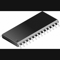
SI9136DB Vishay, SI9136DB Datasheet - Page 13

SI9136DB
Manufacturer Part Number
SI9136DB
Description
Pulse Width Modulation (PWM) Controller IC
Manufacturer
Vishay
Datasheet
1.SI9136LG.pdf
(15 pages)
Specifications of SI9136DB
Silicon Manufacturer
Vishay
Application Sub Type
Power Supply Controller
Kit Application Type
Power Management
Silicon Core Number
SI9136
Kit Contents
Board
Lead Free Status / RoHS Status
Contains lead / RoHS non-compliant
Normal Operation: Buck Converters
In normal operation, the buck converter high-side MOSFET is
turned on with a delay (known as break-before-make time -
t
the high-side MOSFET is turned off and then after a delay
(t
edge of the clock, or the inductor current reaches zero. The
t
guarantee the efficiency is not adversely affected at the high
switching frequency and a specified minimum to account for
variations of possible MOSFET gate capacitances.
During the normal operation, the high-side MOSFET switch
on-time is controlled internally to provide excellent line and
load regulation over temperature. Both buck converters
should have load, line, regulation to within 0.5% tolerance.
Pulse Skipping: Buck Converters
When the buck converter switching frequency is less than the
internal clock frequency, its operation mode is defined as pulse
skipping mode. During this mode, the high-side MOSFET is
turned on until V
its maximum duty ratio. After the high-side MOSFET is turned
off, the low-side MOSFET is turned on after the t
which will remain on until the inductor current reaches zero.
The output voltage will rise slightly above the regulation
voltage after this sequence, causing the controller to stay idle
for the next one, or several clock cycles. When the output
voltage falls slightly below the regulation level, the high-side
MOSFET will be turned on again at the next clock cycle. With
the converter remaining idle during some clock cycles, the
switching losses are reduced in order to preserve conversion
efficiency during the light output current condition.
Current Limit: Buck Converters
When the buck converter inductor current is too high, the
voltage across pin CS3(5) and pin FB3(5) exceeds
approximately 120 mV, the high-side MOSFET would be
turned off instantaneously regardless of the input, or output
condition. The Si9136 features clock cycle by clock cycle
current limiting capability.
Flyback Converter Operation:
Designed mainly for PCMCIA or EEPROM programming, the
Si9136 has a 12-V output non-isolated buck boost converter,
Document Number: 70818
S-00583—Rev. C, 03-Apr-00
BBM
BBM
BBM
), after the rising edge of the clock. After a certain on time,
), the low-side MOSFET is turned on until the next rising
(approximately 25 ns to 60 ns), has been optimized to
CS
-V
FB
reaches 20 mV, or the on time reaches
BBM
delay,
called for brevity a flyback. It consists of two n-channel
MOSFET switches that are turned on and off in phase, and two
diodes. Similar to the buck converter, during the light load
conditions, the flyback converter will switch at a frequency
lower than the internal clock frequency, which can be defined
as pulse skipping mode (PSM); otherwise, it is operating in
normal PWM mode.
Normal Operation: Flyback Converter
In normal operation mode, the two MOSFETs are turned on at
the rising edge of the clock, and then turned off. The on time is
controlled internally to provide excellent load, line, and
temperature regulation. The flyback converter has load, line
and temperature regulation well within 0.5%.
Pulse Skipping: Flyback Converter
Under the light load conditions, similar to the buck converter,
the flyback converter will enter pulse skipping mode. The
MOSFETs will be turned on until the inductor current increases
to such a level that the voltage across the pin CSP and pin CSN
reaches 100 mV, or the on time reaches the maximum duty
cycle. After the MOSFETs are turned off, the inductor current
will conduct through two diodes until it reaches zero. At this
point, the flyback converter output will rise slightly above the
regulation level, and the converter will stay idle for one or
several clock cycle(s) until the output falls back slightly below
the regulation level. The switching losses are reduced by
skipping pulses and so the efficiency during light load is
preserved.
Current Limit: Flyback Converter
Similar to the buck converter; when the voltage across pin CSP
and pin CSN exceeds 410-mV typical, the two MOSFETs will
be turned off regardless of the input and output conditions.
Flyback Lowside Drive
Unlike the gate drive for the two buck converters, the flyback
lowside gate drive DLFY is powered by a voltage that can be
as high as 15 V with 20-V input for the flyback converter. If this
poses concerns on the MOSFET V
resistor-zener circuit can be used: a resistor series with gate
and zener diode across the gate and source to clamp its
voltage. A 100- , 10-V combination works well.
www.vishay.com FaxBack 408-970-5600
Vishay Siliconix
GS
rating, a simple
Si9136
13


