R0K52472VSC000BE Renesas Electronics America, R0K52472VSC000BE Datasheet
R0K52472VSC000BE
Specifications of R0K52472VSC000BE


Related parts for R0K52472VSC000BE


R0K52472VSC000BE Summary of contents
Page 1
To our customers, Old Company Name in Catalogs and Other Documents st On April 1 , 2010, NEC Electronics Corporation merged with Renesas Technology Corporation, and Renesas Electronics Corporation took over all the business of both companies. Therefore, although the ...
Page 2
... Computers; office equipment; communications equipment; test and measurement equipment; audio and visual equipment; home electronic appliances; machine tools; personal electronic equipment; and industrial robots. “High Quality”: Transportation equipment (automobiles, trains, ships, etc.); traffic control systems; anti-disaster systems; anti- crime systems ...
Page 3
Renesas Starter Kit for H8S/2472 User’s Manual RENESAS SINGLE-CHIP MICROCOMPUTER H8S FAMILY Rev.1.00 2008.08 ...
Page 4
By using this Renesas Starter Kit (RSK), the user accepts the following terms. The RSK is not guaranteed to be error free, and the entire risk as to the results and performance of the RSK is assumed by the User. ...
Page 5
Table of Contents Chapter 1. Preface .................................................................................................................................................. 4 Chapter 2. Purpose ................................................................................................................................................. 5 Chapter 3. Power Supply ........................................................................................................................................ 6 3.1. Requirements ............................................................................................................................................... 6 3.2. Power – Up Behaviour ................................................................................................................................. 6 Chapter 4. Board Layout ......................................................................................................................................... 7 4.1. Component Layout ....................................................................................................................................... ...
Page 6
Cautions This document may be, wholly or partially, subject to change without notice. All rights reserved. Duplication of this document, either in whole or part is prohibited without the written permission of Renesas Technology Europe Limited. Trademarks All brand or ...
Page 7
This RSK is an evaluation tool for Renesas microcontrollers. This manual describes the technical details of the RSK hardware. The Quick Start Guide and Tutorial Manual provide details of the software installation and debugging environment. Features include: • Renesas Microcontroller ...
Page 8
Chapter 3. Power Supply 3.1. Requirements This RSK operates from a 5V power supply. A diode provides reverse polarity protection only if a current limiting power supply is used. All RSK boards are supplied with an E10A debugger. This product ...
Page 9
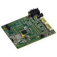
Component Layout The following diagram shows top layer component layout of the board. Application board interface JA5 LCD Display LCD Microcontroller pin headers USB Ethernet Chapt er 4. Board Layout JA1 MCU J3 J4 JA6 ...
Page 10
Board Dimensions The following diagram gives the board dimensions and connector positions. All through hole connectors are on a common 0.1” grid for easy interfacing. 86.36mm Short Board = 85 mm 50.80 mm 43.18 mm 35.56 mm 27.00mm SW ...
Page 11
Chapter 5. Block Diagram Figure 5-1 shows the CPU board components and their connectivity. Figure 5-2 shows the connections to the RSK. Figure 5-1: Block Diagram Figure 5-2: RSK Connections 9 ...
Page 12
Chapter 6. User Circuitry 6.1. Switches There are four switches located on the CPU board. The function of each switch and its connection are shown in Table 6-1. Switch RES When pressed, the RSK microcontroller is reset. SW1/BOOT* Connects to ...
Page 13
Description Function SCIF Default serial port SCIF Default serial port SCI3 Spare Serial Port SCI3 Spare Serial Port The SCIF port is also availab le on J7/J8 and JA2. The SCI3 port is available on J5/J6 and JA6. 6.5.U SB ...
Page 14
Description RM_REF-CLK RM_TX-EN RM_TXD1 RM_TXD0 RM_CRS-DV RM_RXD1 RM_RXD0 RM_RX-ER MDC MDIO LINKSTA_A22 WOL 6.7.Debug LCD Mod A debug LCD module is supplied Care should be taken to ensure the pins are inserted correctly into LCD. The debug ...
Page 15
Option Links Table 6-7 below describes the function of the option links contained on this RS default configuration is indicate d by BOLD text Reference Func tion R15 Serial Po rt Configuration R19 Serial Po rt configura tion R28 ...
Page 16
Reference Function R56 Application board interface R60 Application board interface R69 Application board interface R95 Application board interfa ce R96 Application board interfa ce R114 Application board interface R115 Application board interface R116 Application board interface Table 6-9 b elow ...
Page 17
Reference Function R125 Power sourc e R126 MCU power supply R127 Ground R128 Power sourc e R129 Power sourc e R130 Power source R131 Power source R153 Power source R154 Power source R155 Pow er source R156 Power source R157 ...
Page 18
Reference Function R93 Clock Oscillator R94 Clock Oscillator R98 Clock Oscillator R99 Clock Oscillator R100 Clock Oscillator R101 Clock Oscillator R102 Clock Oscillator R103 Clock Oscillator R105 Clock Oscillator R199 Clock Oscillator Table 6-12 below describes the function of the ...
Page 19
Reference Function R46 Analog Voltage Source R189 Analog Voltage Source R198 Analog Voltage Source Table 6-14 below describes the function of the option links associated with MCU modes. The default configuration is indicated by BOLD text. Reference Function R160 MCU ...
Page 20
Reset Circuit The C PU Board inc ludes a simple la tch circuit that links the mode selection and reset the de vice b etween Boot Mode and U evaluation of the op erating m odes of requir ements ...
Page 21
This RSK supports Boot mode, User Boot mode, User Program Mode and User mode. Details of programming the FLASH memory is described in the H8S/2472 Group Hardware Manual. 7.1.User Boot mode Refer to H8S/2472 Group Hardware Man user Boot Mode ...
Page 22
... Chapter 8. Pro The board is intended for use with HEW and the supplied E10A debugger. Refer to H8S programming the microcontroller without using these tools. Please note that to use E10A debugger, ju gramming M ethods /2472 Group Hardware Manual for details of 20 mper E10A_EN must be fitted. ...
Page 23
Microcontroller Headers Table 9-1 to Table 9-8 show the microcontroller pin headers and their corresponding microcontroller connections. The header pins connect directly to the microcontroller pin unless otherwise stated. Pin Circuit Net Name 1 UC_VCC 3 CON_XTAL 5 GROUND ...
Page 24
Pin Circuit Net Name 1 WRn_HWRn 3 A15 5 A13 UC_VCC 11 PIN_C6 D13 RM_TXD1 23 RM_CRS-DV 25 GROUND Pin Circuit Net Name 1 PIN_E15 ...
Page 25
Pin Circuit Net Name 1 PIN_E13 3 GROUND 5 LED0 7 TDO 9 GROUND 11 BOARD_VCC 13 IRQ10n Pin Circuit Net Name 1 AN6 3 AN4 5 AN1 IO2 11 IO5 13 PIN_R9 15 PIN_R8 17 PIN_R7 ...
Page 26
Pin Circuit Net Name ON_AVREF 5 AN7 7 AD POT_A N0 9 IO3 11 IO6 13 PIN_N9 15 PIN_N8 PIN_N6 21 ADTRGn_TxD3 A18 27 UC_V CC 29 LINKSTA_A22 Pin Circuit ...
Page 27
Pin Circuit Net Name DLCDRS 5 PIN_J3 7 EXPWX0 9 CS256n PIN_E3 J8 Device Pin Circuit Net Name Pin L3 2 DLCDD5 K3 4 LWRn J3 6 AHn H3 8 EXPWX1 G3 10 RxD0 ...
Page 28
Headers Table 9-9 to Table 9-13 below show the standard application head er connections. Pin Generic Header Name CON_5V CON_3V3 5 A VCC CON_AVCC 7 A Vref CON_AVREF AN0 11 ...
Page 29
Pin Generic Header Name Signal Name 1 AD4 AN4 3 AD6 AN6 5 CAN1TX CAN2TX NC 9 AD8 NC 11 AD10 NC 13 TIOC0A NC 15 TIOC TCLKC NC 19 M2_Up NC 21 M2_Vp ...
Page 30
Pin Generic Header Name CPU board Signal Name A10 A10 13 A12 A12 15 A14 A14 ...
Page 31
... Chapter 10. Code Development 10.1. Overview Note: For all code debugging using Renesas software tools, the RSK board must be connected USB port via an E10A. An E10A pod is supplied with the RSK product ompiler Re str The compiler supplied with this RSK is fully functional for a period of 60 days from first use. After the first 60 days of use have expired, the compiler will default to a maximum of 64k code and data ...
Page 32
Memory Map Figure 10-1: Memory Map 30 ...
Page 33
Chapter 11.Component Placement Figure 11-1: Component Placement – Front view 31 ...
Page 34
... For information about the H8S/2472 assembly language, refer to the H8S Series Software Manual. Online technical support and information is available at: Technical Contact Details America: techsupport.rta@renesas.com Europe: tools.support.eu@renesas.com Japan: csc@renesas.com General information on Renesas Microcontrollers can be found on the Renesas website at: r 12. Additional Information http://www.renesas.com/renesas_starter_kits 32 http://www ...
Page 35
Renesas Starter Kit for H8S/2472 User's Manual Publication Date Rev.1.00 28.08.2008 Published by: Renesas Technology Europe Ltd. Duke’s Meadow, Millboard Road, Bourne End Buckinghamshire SL8 5FH, United Kingdom ©2008 Renesas Technology Europe and Renesas Solutions Corp., All Rights Reserved. ...
Page 36
Renesas Starter Kit for H8S/2472 1753, Shimonumabe, Nakahara-ku, Kawasaki-shi, Kanagawa 211-8668 Japan User’s Manual REG10J0082-0100 ...