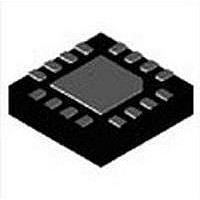
MAX17149ETE+ Maxim Integrated Products, MAX17149ETE+ Datasheet - Page 2

MAX17149ETE+
Manufacturer Part Number
MAX17149ETE+
Description
LED Drivers 6-String WLED Driver
Manufacturer
Maxim Integrated Products
Datasheet
1.MAX17129ETE.pdf
(20 pages)
Specifications of MAX17149ETE+
Operating Supply Voltage
3 V to 26 V
Maximum Supply Current
4 mA
Maximum Power Dissipation
1176 mW
Maximum Operating Temperature
+ 85 C
Mounting Style
SMD/SMT
Package / Case
TQFN-16
Minimum Operating Temperature
- 40 C
Lead Free Status / RoHS Status
Lead free / RoHS Compliant
Low-Cost, 6-String WLED Drivers with
Quick-PWM Step-Up Converter
ABSOLUTE MAXIMUM RATINGS
FSEL, IN, BRT, EN to GND ..................................-0.3V to +28V
FB_, LX, OVP to PGND .........................................-0.3V to +48V
PGND to GND ......................................................-0.3V to +0.3V
V
ISET to GND ............................................... -0.3V to VCC + 0.3V
LX Switch Continuous RMS Current .....................................1.6A
Continuous Power Dissipation (T
Stresses beyond those listed under “Absolute Maximum Ratings” may cause permanent damage to the device. These are stress ratings only, and functional
operation of the device at these or any other conditions beyond those indicated in the operational sections of the specifications is not implied. Exposure to absolute
maximum rating conditions for extended periods may affect device reliability.
ELECTRICAL CHARACTERISTICS
(Circuit of Figure 1. V
2
IN Input Voltage Range
IN Standby Current
V
V
V
IN UVLO Threshold
STEP-UP CONVERTER
LX On-Resistance
LX Leakage Current
Off-Time
LX Peak Current Limit
Minimum On-Time
INPUT LEAKAGE/BIAS CURRENTS
EN Bias Current
BRT Bias Current
EN Input Impedance
OVP Input Current
CC
16-Pin Thin QFN (derate 14.7mW/NC above +70NC) .. 1176mW
CC
CC
CC
to GND .............................................................-0.3V to +6V
Output Voltage
Current Limit
UVLO Threshold
PARAMETER
IN
= 12V, R
ISET
A
= +70NC)
IN not connected to V
IN connected to V
V
V
V
V
Rising edge, typical hysteresis = 100mV
Rising edge, typical hysteresis = 200mV; IN not con-
nected to V
100mA from LX to PGND
V
FSEL = GND, V
FSEL = V
Duty cycle = 75%
0.3V < V
4.1V < V
0.3V < V
4.1V < V
V
= 100kI, T
EN
EN
EN
CC
LX
OVP
= 40V, T
= 3V, V
= 0V, V
= 3V, 0 < I
is forced to 3.5V; IN not connected to V
= 40V, V
EN
EN
BRT
BRT
CC
A
CC
< 3.5V, T
< 28V, T
IN
IN
, V
A
< 3.5V, T
< 28V, T
= 0°C to +85°C, unless otherwise noted. Typical values are at T
= 26V, no external loads
= 26V
FB
= +25NC
IN
VCC
IN
= 12V, V
= 0.75V
CC
= 12V, V
< 10mA
A
A
CONDITIONS
A
CC
A
= +25NC
= +25NC
= +25NC
= +25NC
OVP
OVP
= 22V
= 22V
Operating Temperature Range .......................... -40NC to +85NC
Junction Temperature .....................................................+150NC
Storage Temperature Range ............................ -60NC to +150NC
ESD
Lead Temperature (soldering, 10s) ................................+300NC
Soldering Temperature (reflow) ......................................+260NC
HBM .................................................................................±2kV
MM ................................................................................ ±200V
CC
2.65
MIN
450
900
750
6.2
3.0
3.6
5.5
2.5
15
1000
1500
TYP
5.75
0.05
250
500
3.2
0.1
3.8
2.8
30
50
15
3
A
= +25NC.) (Note 1)
MAX
1100
2000
500
550
100
110
5.5
4.0
2.9
3.5
26
45
15
50
4
5
6
1
6
UNITS
mI
mA
mA
kI
FA
FA
FA
FA
FA
ns
ns
V
V
V
V
A


