TSL210 TAOS, TSL210 Datasheet - Page 3
TSL210
Manufacturer Part Number
TSL210
Description
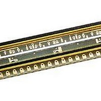
Photodiodes Linear Array 200 DPI
Manufacturer
TAOS
Type
Linear Sensor Arrayr
Datasheet
1.TSL210.pdf
(12 pages)
Specifications of TSL210
Maximum Operating Temperature
+ 70 C
Minimum Operating Temperature
0 C
Lead Free Status / RoHS Status
Lead free / RoHS Compliant


TSL210
640 × 1 LINEAR SENSOR ARRAY
TAOS039B − MAY 2007
The output and reset of the integrators in each section are controlled by a 128-bit shift register and reset logic.
An output cycle is initiated by clocking in a logic 1 on SI. As the SI pulse is clocked through the shift register,
the charge stored on the sampling capacitors of each pixel is sequentially connected to a charge-coupled output
amplifier that generates a voltage on analog output AO (given above). After being read, the pixel integrator is
th
then reset, and the next integration period begins for that pixel. On the 129
clock rising edge, the SO pulse
is clocked out on SO signifying the end of the read cycle. The section is then ready for another read cycle. The
SO of each section can be connected to SI on the next section in the array (Figure 4). SO can be used to signify
the read is complete.
AO is driven by a source follower that requires an external pulldown resistor (330-Ω typical). The output is
nominally 0 V for no light input, 2 V for normal white-level, and 3.4 V for saturation light level. When the device
is not in the output phase, AO is in a high impedance state.
A 0.1 μF bypass capacitor should be connected between V
and ground as close as possible to the device.
DD
The LUMENOLOGY r Company
Copyright E 2007, TAOS Inc.
r
r
www.taosinc.com
3
Related parts for TSL210
Image
Part Number
Description
Manufacturer
Datasheet
Request
R

Part Number:
Description:
Microcontroller Modules & Accessories TAOS Eval Module w/USB Interface
Manufacturer:
TAOS
Part Number:
Description:
Optical Sensor Development Tools TAOS Eval Module
Manufacturer:
TAOS

Part Number:
Description:
Industrial Optical Sensors Ambient Light Sensor SMBus
Manufacturer:
TAOS
Datasheet:

Part Number:
Description:
Photodiodes TriColor Sensor RGB, Clear Ch
Manufacturer:
TAOS
Datasheet:

Part Number:
Description:
LED Displays Hexadecimal Display 4-bit
Manufacturer:
TAOS
Datasheet:

Part Number:
Description:
Photodiodes Linear Sensor Array 200dpi 64pix
Manufacturer:
TAOS
Datasheet:

Part Number:
Description:
Industrial Optical Sensors Ambient Light Sensor SMBus
Manufacturer:
TAOS
Datasheet:

Part Number:
Description:
Photodiodes Linear Array 200 DPI
Manufacturer:
TAOS
Datasheet:

Part Number:
Description:
Photodiodes Light to Voltage Converter
Manufacturer:
TAOS
Datasheet:

Part Number:
Description:
Photodiodes Linear Array 200 DPI
Manufacturer:
TAOS
Datasheet:
Part Number:
Description:
Industrial Optical Sensors Ambient Light Sensor SMBus
Manufacturer:
TAOS
Datasheet:
Part Number:
Description:
Photodiodes TriColor Sensor RGB, Clear Ch
Manufacturer:
TAOS
Datasheet:
Part Number:
Description:
LED Displays Hexadecimal Display 4-bit
Manufacturer:
TAOS
Datasheet:
Part Number:
Description:
Photodiodes Linear Sensor Array 200dpi 64pix
Manufacturer:
TAOS
Datasheet:
