B32523-Q6155-M EPCOS Inc, B32523-Q6155-M Datasheet
B32523-Q6155-M
Specifications of B32523-Q6155-M


Related parts for B32523-Q6155-M


B32523-Q6155-M Summary of contents
Page 1
... Film Capacitors Metallized Polyester Film Capacitors (MKT) Series/Type: B32520 ... B32529 Date: May 2009 © EPCOS AG 2009. Reproduction, publication and dissemination of this publication, enclosures hereto and the information contained therein without EPCOS' prior express consent is prohibited. ...
Page 2
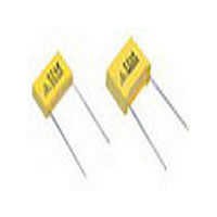
... Dimensional drawing Dimensions in mm Lead spacing Lead diameter 0 5.0 0.5 7.5 0.5 10.0 0.6 1) 15.0 0.8 22.5 0.8 27.5 0.8 37.5 1.0 1) 0.5 mm for capacitor width Page B32520 ... B32529 Type B32529 B32520 B32521 B32522 B32523 B32524 B32526 ...
Page 3
... Technology Stacked-film technology / w = Wound capacitor technology Please read Important notes at the end of this document. General purpose (stacked/wound) 7.5 mm B32520 100 250 400 63 63 160 200 40 Page B32520 ...
Page 4
... Technology Stacked-film technology / w = Wound capacitor technology Please read Important notes at the end of this document. 22.5 mm B32523 100 250 400 630 63 63 160 200 200 40 Page 27.5 mm B32524 100 250 400 630 ...
Page 5
... Overview of available types Lead spacing 37.5 mm Type B32526 Page 20 Technology DC AC) 40 RMS 3.3 4.7 6 100 150 220 Technology Stacked-film technology / w = Wound capacitor technology Please read Important notes at the end of this document. B32520 ... B32529 General purpose (stacked/wound 100 250 63 160 Page 400 200 ...
Page 6
B32529 General purpose (stacked) Ordering codes and packing units (lead spacing 5 mm Max. dimensions R RMS 0.0010 2.5 0.0015 2.5 0.0022 2.5 ...
Page 7
Ordering codes and packing units (lead spacing 5 mm Max. dimensions R RMS 100 63 0.0010 2.5 0.0015 2.5 0.0022 2.5 0.0033 2.5 0.0047 2.5 ...
Page 8
B32529 General purpose (stacked) Ordering codes and packing units (lead spacing 5 mm Max. dimensions R RMS 250 160 0.0010 2.5 0.0015 2.5 0.0022 2.5 ...
Page 9
Ordering codes and packing units (lead spacing 5 mm Max. dimensions R RMS 400 200 0.0010 2.5 0.0015 2.5 0.0022 2.5 0.0033 2.5 0.0047 2.5 ...
Page 10
B32520 General purpose (stacked) Ordering codes and packing units (lead spacing 7.5 mm Max. dimensions R RMS 0.068 2.5 0.10 2.5 0.15 2.5 ...
Page 11
Ordering codes and packing units (lead spacing 7.5 mm Max. dimensions R RMS 400 200 0.0010 2.5 0.0015 2.5 0.0022 2.5 0.0033 2.5 0.0047 2.5 ...
Page 12
B32521 General purpose (stacked/wound) Ordering codes and packing units (lead spacing 10 mm Max. dimensions R RMS 0.47 4.0 0.68 4.0 1.0 4.0 1.5 ...
Page 13
Ordering codes and packing units (lead spacing 10 mm Max. dimensions R RMS 630 200 0.0068 4.0 0.010 4.0 0.015 5.0 0.022 5.0 0.033 6.0 Wound ...
Page 14
B32522 General purpose (stacked/wound) Ordering codes and packing units (lead spacing 15 mm Max. dimensions R RMS 0.68 5.0 1.0 5.0 1.5 5.0 2.2 ...
Page 15
Ordering codes and packing units (lead spacing 15 mm Max. dimensions R RMS 250 160 0.10 5.0 0.15 5.0 0.22 5.0 0.33 5.0 0.47 6.0 0.68 ...
Page 16
B32522 General purpose (stacked/wound) Ordering codes and packing units (lead spacing 15 mm Max. dimensions R RMS 630 200 0.033 5.0 0.047 5.0 0.068 6.0 0.10 ...
Page 17
... B32523Q3105+*** 2720 16.0 26.5 B32523Q3155+*** 2320 16.5 26.5 B32523Q3225+*** 1560 20.5 26.5 B32523Q3335+*** 1480 15.0 26.5 B32523Q6224+*** 2720 15.0 26.5 B32523Q6334+*** 2720 16.0 26.5 B32523Q6474+*** 2320 16.5 26.5 B32523Q6684+*** 1920 16.5 26.5 B32523Q6105+*** 1560 20.5 26.5 B32523Q6155+*** 1480 15.0 26.5 B32523Q8104+*** 2720 15 ...
Page 18
B32524 General purpose (wound) Ordering codes and packing units (lead spacing 27.5 mm Max. dimensions R RMS 4.7 11.0 6.8 11.0 10 11.0 ...
Page 19
Ordering codes and packing units (lead spacing 27.5 mm Max. dimensions R RMS 400 200 0.68 11.0 1.0 11.0 1.5 11.0 2.2 11.0 3.3 14.0 ...
Page 20
B32526 General purpose (wound) Ordering codes and packing units (lead spacing 37.5 mm Max. dimensions R RMS 12.0 33 12.0 47 12.0 ...
Page 21
Technical data Operating temperature range Dissipation factor tan ( (upper limit values) Insulation resistance R ins or time constant = ins rel. humidity 65% (minimum as-delivered values) ...
Page 22
B32520 ... B32529 General purpose (stacked/wound) Pulse handling capability "dV/dt" represents the maximum permissible voltage change per unit of time for non-sinusoidal voltages, expressed "k " represents the maximum permissible pulse characteristic of the waveform applied to ...
Page 23
Impedance Z versus frequency f (typical values) Please read Important notes at the end of this document. B32520 ... B32529 General purpose (stacked/wound) Page ...
Page 24
B32529 General purpose (stacked) Permissible AC voltage V RMS For T >55 C, please refer to "General technical information", section 3.2.3. A Lead spacing DC/ 100 V DC/ Please read Important notes ...
Page 25
Permissible AC voltage V RMS For T >55 C, please refer to "General technical information", section 3.2.3. A Lead spacing 5 mm 400 V DC/200 V AC Please read Important notes at the end of this document. General purpose (stacked) ...
Page 26
B32520 General purpose (stacked) Permissible AC voltage V RMS For T >55 C, please refer to "General technical information", section 3.2.3. A Lead spacing 7 DC/ 250 V DC/160 V AC Please read Important notes ...
Page 27
Permissible AC voltage V RMS For T >55 C, please refer to "General technical information", section 3.2.3. A Lead spacing DC/ 250 V DC/160 V AC Please read Important notes at the end of ...
Page 28
B32521 General purpose (stacked/wound) Permissible AC voltage V RMS For T >55 C, please refer to "General technical information", section 3.2.3. A Lead spacing 10 mm 630 V DC/200 V AC Please read Important notes at the end of this ...
Page 29
Permissible AC voltage V RMS For T >55 C, please refer to "General technical information", section 3.2.3. A Lead spacing DC/ 250 V DC/160 V AC Please read Important notes at the end of ...
Page 30
B32522 General purpose (stacked/wound) Permissible AC voltage V RMS For T >55 C, please refer to "General technical information", section 3.2.3. A Lead spacing 15 mm 450 V DC/200 V AC Please read Important notes at the end of this ...
Page 31
... Permissible AC voltage V RMS For T >55 C, please refer to "General technical information", section 3.2.3. A Lead spacing 22 DC/ 250 V DC/160 V AC Please read Important notes at the end of this document. General purpose (wound) versus frequency f (for sinusoidal waveforms, T 100 V DC/ 400 V DC/200 V AC Page B32523 ...
Page 32
... B32523 General purpose (wound) Permissible AC voltage V RMS For T >55 C, please refer to "General technical information", section 3.2.3. A Lead spacing 22.5 mm 630 V DC/200 V AC Please read Important notes at the end of this document. versus frequency f (for sinusoidal waveforms, T Page ...
Page 33
Permissible AC voltage V RMS For T >55 C, please refer to "General technical information", section 3.2.3. A Lead spacing 27 DC/ 250 V DC/160 V AC Please read Important notes at the end of ...
Page 34
B32524 General purpose (wound) Permissible AC voltage V RMS For T >55 C, please refer to "General technical information", section 3.2.3. A Lead spacing 27.5 mm 630 V DC/220 V AC Please read Important notes at the end of this ...
Page 35
Permissible AC voltage V RMS For T >55 C, please refer to "General technical information", section 3.2.3. A Lead spacing 37 DC/ 250 V DC/160 V AC Please read Important notes at the end of ...
Page 36
... Before a solderability test is carried out, terminals are subjected to accelerated ageing (to IEC 60068-2-2, test Ba exposure to dry heat at 155 C). Since the ageing temperature is far higher than the upper category temperature of the capacitors, the terminal wires should be cut off from the capacitor before the ageing procedure to prevent the solderability being impaired by the products of any capacitor decomposition that might occur ...
Page 37
... Please read Important notes at the end of this document. General purpose (stacked/wound) 2.0 +0/ 0.5 mm from capacitor body or seating plane Heat-absorbing board, (1.5 0.5) mm thick, between capacitor body and liquid solder No visible damage 2% for MKT/MKP/MFP 5% for EMI suppression capacitors As specified in sectional specification Page B32520 ... B32529 ...
Page 38
... B32520 ... B32529 General purpose (stacked/wound) 1.3 General notes on soldering Permissible heat exposure loads on film capacitors are primarily characterized by the upper cate- gory temperature T . Long exposure to temperatures above this type-related temperature limit max can lead to changes in the plastic dielectric and thus change irreversibly a capacitor's electrical characteristics ...
Page 39
... MKT, MKP, MFP (coated/boxed) Even when suitable solvents are used, a reversible change of the electrical characteristics may occur in uncoated capacitors immediately after they are washed. Thus it is always recommended to dry the components (e. before they are subjected to subsequent electrical test- ing. Table A ...
Page 40
... B32520 ... B32529 General purpose (stacked/wound) 3 Embedding of capacitors in finished assemblies In many applications, finished circuit assemblies are embedded in plastic resins. In this case, both chemical and thermal influences of the embedding ("potting") and curing processes must be taken into account. Our experience has shown that the following potting materials can be recommended: non-flexible epoxy resins with acid-anhydride hardeners ...
Page 41
... The capacitors are tested to IEC 60068-2-6. EPCOS offers film capacitors specially designed for operation under more severe vibration regimes such as those found in automotive applications. Consult our catalog "Film Capacitors for Automotive Electronics". Please read Important notes at the end of this document. B32520 ... B32529 ...
Page 42
... Topic Safety information Soldering Do not exceed the specified time or temperature limits during soldering. Cleaning Use only suitable solvents for cleaning capacitors. 2 "Cleaning" Embedding of When embedding finished circuit assemblies in capacitors in plastic resins, chemical and thermal influences finished assemblies must be taken into account. ...
Page 43
Symbols and terms Symbol English Heat transfer coefficient Temperature coefficient of capacitance C A Capacitor surface area Humidity coefficient of capacitance C C Capacitance C Rated capacitance R C Absolute capacitance change C/C Relative capacitance change (relative deviation of actual ...
Page 44
B32520 ... B32529 General purpose (stacked/wound) Symbol English I (Sinusoidal) alternating current, RMS root-mean-square value i Capacitance drift z k Pulse characteristic 0 L Series inductance S Failure rate Constant failure rate during useful 0 service life Failure rate, determined ...
Page 45
Symbol English V Category voltage C V Category AC voltage C,RMS V Corona-discharge onset voltage CD V Charging voltage voltage DC V Fly-back capacitor voltage FB V Input voltage i V Output voltage o V Operating voltage ...
Page 46
Important notes The following applies to all products named in this publication: 1. Some parts of this publication contain statements about the suitability of our products for certain areas of application. These statements are based on our knowledge of typical ...