IL352 Vishay, IL352 Datasheet
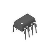
Transistor Output Optocouplers Phototransistor Out Single CTR >100%

IL352

Manufacturer Part Number
IL352
Description
Transistor Output Optocouplers Phototransistor Out Single CTR >100%
Manufacturer
Vishay
Datasheet

Specifications of IL352

Isolation Voltage
3000 Vrms
Maximum Input Diode Current
60 mA
Maximum Reverse Diode Voltage
6 V
Output Device
Phototransistor
Output Type
DC
Configuration
1 Channel
Input Type
DC
Maximum Collector Emitter Voltage
70 V
Maximum Collector Emitter Saturation Voltage
0.3 V
Maximum Forward Diode Voltage
1.5 V
Maximum Collector Current
100 mA
Maximum Power Dissipation
50 mW
Maximum Operating Temperature
+ 85 C
Minimum Operating Temperature
- 40 C
Package / Case
SOP-7
No. Of Channels
1
Optocoupler Output Type
Phototransistor
Input Current
10mA
Output Voltage
30V
Opto Case Style
SMD
No. Of Pins
8
Input Current Max
10mA
Mounting Type
Through Hole
Rohs Compliant
Yes
Lead Free Status / RoHS Status
Lead free / RoHS Compliant

Available stocks

Company
Part Number
Manufacturer
Quantity
Price
Part Number:
IL3522
Manufacturer:
NVE
Quantity:
20 000
Part Number:
IL3522E
Manufacturer:
NVE
Quantity:
20 000
IL352
Vishay Semiconductors
DESCRIPTION
The IL352 optically coupled isolator that features a high
current transfer ratio, low coupling capacitance and high
isolation voltage. It has a GaAs infrared emitting diode
emitter, which is optically coupled to a silicon planar
phototransistor detector. The component is housed in a thin
line package.
The coupling device is designed for signal transmission
between two electrically separated circuits. The potential
difference between the circuits to be coupled must not
exceed the maximum permissible reference voltages.
Notes
(1)
(2)
www.vishay.com
370
ORDER INFORMATION
PART
IL352
ABSOLUTE MAXIMUM RATINGS
PARAMETER
INPUT
Reverse voltage
DC forward current
Total power dissipation
Derate linearly from 25 °C
OUTPUT
Collector emitter voltage
Emitter base voltage
Collector current
Total power dissipation
Derate linearly from 25 °C
COUPLER
Isolation test voltage
between emitter and detector
Isolation resistance
Storage temperature range
Ambient temperature range
Junction temperature
Soldering temperature
T
Stresses in excess of the absolute maximum ratings can cause permanent damage to the device. Functional operation of the device is not
implied at these or any other conditions in excess of those given in the operational sections of this document. Exposure to absolute maximum
ratings for extended periods of the time can adversely affect reliability.
Refer to reflow profile for soldering conditions for surface mounted devices.
i179027
amb
Optocoupler, Phototransistor Output, with Base Connection
= 25 °C, unless otherwise specified.
(2)
For technical questions, contact: optocoupler.answers@vishay.com
N.C
N.C
C
A
V
V
distance to seating plane
max. 10 s, dip soldering:
IO
1
IO
2
3
4
= 500 V, T
TEST CONDITION
= 500 V, T
(1)
≥ 1.5 mm
t ≤ 1 ms
t = 1.0 s
amb
amb
8
7
6
5
= 100 °C
= 25 °C
B
C
E
FEATURES
• Good CTR linearly depending on forward
• Isolation test voltage: 3000 V
• High collector emitter voltage, V
• Low saturation voltage
• Fast switching times
• Lead (Pb)-free component
• Component in accordance to RoHS 2002/95/EC and
AGENCY APPROVALS
• UL1577, file no. E52744 system code S
• DIN EN 60747-5-5 (VDE 0884) available with option 1
current
WEEE 2002/96/EC
SYMBOL
V
P
P
T
V
V
T
T
R
R
V
EBO
I
I
amb
I
diss
diss
T
ISO
CE
stg
C
C
sld
F
IO
IO
R
j
CTR > 100 %, SMD-8
- 40 to + 150
REMARKS
- 40 to + 85
VALUE
≥ 10
≥ 10
3000
0.66
100
150
100
260
2.5
60
50
70
50
6
7
12
11
RMS
CEO
Document Number: 83624
= 30 V
Rev. 1.6, 10-Dec-08
mW/°C
mW/°C
UNIT
V
mW
mW
mA
mA
mA
°C
°C
°C
°C
RMS
Ω
Ω
V
V
V

Related parts for IL352

IL352 Summary of contents

Page 1

... N.C C N.C i179027 DESCRIPTION The IL352 optically coupled isolator that features a high current transfer ratio, low coupling capacitance and high isolation voltage. It has a GaAs infrared emitting diode emitter, which is optically coupled to a silicon planar phototransistor detector. The component is housed in a thin line package ...

Page 2

... MAX. V 1 CEO BV 7 ECO CEO I 500 CEO BV 70 CBO 0.3 CEsat 0.5 IO MIN. TYP. MAX. CTR 100 DC CTR 34 DC MIN. TYP. MAX. 10 off 100 Ω kHz iil352_02 Fig Switching Schematic IL352 UNIT V µ µ UNIT % % UNIT µs www.vishay.com 371 ...

Page 3

... NCTR(SAT) NCTR 0.0 0 LED Current - iil352_06 LED Current 1.5 Normalized to mA ° CTRce(sat 0 1 °C A 0.5 NCTR(SAT) NCTR 0.0 0 LED Current - mA F iil352_07 LED Current ° ° °C 85 ° LED Current - mA F iil352_08 Document Number: 83624 Rev. 1.6, 10-Dec-08 100 100 60 ...

Page 4

... Vishay Semiconductors 10 Normalized to mA ° NIb °C A 0.1 NIb °C A NIb °C A NIb °C A 0.01 0 iil352_12 I - LED Current - mA F and Temperature F 1000 ° 1 pHL 100 10 t pLH 1 0 Collector Load Resistor (kΩ) L iil352_13 www.vishay.com IL352 100 2.5 2.0 1.5 1.0 100 373 ...

Page 5

... IL352 Vishay Semiconductors PACKAGE DIMENSIONS in inches (millimeters) Pins 6 and 7 0.230 (5.84) 0.224 (5.69) ISO method A 0.040 (1.02) 0.036 (0.91) 0.050 (1.27) typ. www.vishay.com For technical questions, contact: optocoupler.answers@vishay.com 374 Optocoupler, Phototransistor Output, with Base Connection 0.224 (5.7) 0.050 (1.27) 0.346 (8.79) ...

Page 6

... Vishay Semiconductor GmbH, P.O.B. 3535, D-74025 Heilbronn, Germany Document Number: 83624 For technical questions, contact: optocoupler.answers@vishay.com Rev. 1.6, 10-Dec-08 Optocoupler, Phototransistor Output, with Base Connection and may do so without further notice. IL352 Vishay Semiconductors www.vishay.com 375 ...

Page 7

... Vishay disclaims any and all liability arising out of the use or application of any product described herein or of any information provided herein to the maximum extent permitted by law. The product specifications do not expand or otherwise modify Vishay’ ...

Related keywords