LPC-MT-2106 Olimex Ltd., LPC-MT-2106 Datasheet
LPC-MT-2106
Specifications of LPC-MT-2106
Available stocks


Related parts for LPC-MT-2106


LPC-MT-2106 Summary of contents
Page 1
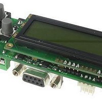
... LPC-MT-2106 DEVELOPMENT BOARD FOR LPC2106 ARM7TDMI-S MICROCONTROLLER Features: MCU: 16/32 bit LPC2106 with 128K Bytes Program Flash, 64K Bytes RAM, RTC, 2x UARTs, I2C, SPI, 2x 32bit TIMERS, 7x CCR, 6x PWM, WDT, 5V tolerant I/ 60MHz operation standard JTAG connector with ARM 2x10 pin layout for programming/debugging with ...
Page 2
... PIN10 thus allows P0 used either for Buzzer either for RS232 TX1 available in extension port header. Oscillator: 14.7456 Mhz crystal is used for LPC2106 as it allows easy setup on any communication speed This makes programming with Philips ISP utility possible http://www.olimex.com/dev ...
Page 3
... Flash to run. Copyright(c) 2004, OLIMEX Ltd., All rights reserved. Development boards for ARM, AVR, MSP430 and PIC microcontrollers Board layout front: Board layout back: Ordering codes: LPC-MT-2106 - assembled and tested with LPC2106 microcontroller http://www.olimex.com/dev ...
Page 4
...