DF10S-E3/45 Vishay, DF10S-E3/45 Datasheet - Page 3
DF10S-E3/45
Manufacturer Part Number
DF10S-E3/45
Description
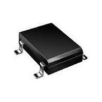
DIODE GPP 1A 1000V 4SMD
Manufacturer
Vishay
Datasheet
1.DF005S-E345.pdf
(4 pages)
Specifications of DF10S-E3/45
Voltage - Peak Reverse (max)
1000V
Current - Dc Forward (if)
1A
Diode Type
Single Phase
Speed
Standard Recovery >500ns, > 200mA (Io)
Mounting Type
Surface Mount
Package / Case
4-SMD (DFS)
Product
Single Phase Bridge
Peak Reverse Voltage
1000 V
Maximum Rms Reverse Voltage
700 V
Forward Continuous Current
1 A
Max Surge Current
50 A
Forward Voltage Drop
1.1 V
Maximum Reverse Leakage Current
5 uA
Maximum Operating Temperature
+ 150 C
Length
8.51 mm
Width
6.5 mm
Height
3.3 mm
Mounting Style
SMD/SMT
Minimum Operating Temperature
- 55 C
No. Of Phases
Single
Repetitive Reverse Voltage Vrrm Max
1kV
Forward Current If(av)
1A
Forward Voltage Vf Max
1.1V
Diode Mounting Type
SMD
Operating Temperature Range
-55°C To +150°C
Phase Type
Single Phase
Number Of Elements
1
Peak Rep Rev Volt
1kV
Rms Voltage (max)
700V
Peak Non-repetitive Surge Current (max)
50A
Avg. Forward Curr (max)
1@Ta=40CA
Rev Curr
5uA
Forward Voltage
1.1V
Package Type
Case DFS
Operating Temp Range
-55C to 150C
Pin Count
4
Mounting
Surface Mount
Operating Temperature Classification
Military
Lead Free Status / RoHS Status
Lead free / RoHS Compliant
Reverse Recovery Time (trr)
-
Lead Free Status / Rohs Status
Compliant
Other names
DF10S-E3/77
Available stocks
Company
Part Number
Manufacturer
Quantity
Price


PACKAGE OUTLINE DIMENSIONS in inches (millimeters)
Document Number: 88573
Revision: 30-Jan-08
Figure 4. Typical Reverse Leakage Characteristics Per Diode
0.01
0.01
100
0.1
0.1
10
Figure 3. Typical Forward Characteristics Per Diode
10
1
1
0.4
0
Percent of Rated Peak Reverse Voltage (%)
Instantaneous Forward Voltage (V)
0.6
20
T
J
0.320 (8.13)
0.335 (8.51)
0.205 (5.2)
T
0.195 (5.0)
= 125 °C
J
0.8
40
= 50 °C
PDD-Americas@vishay.com, PDD-Asia@vishay.com, PDD-Europe@vishay.com
For technical questions within your region, please contact one of the following:
T
Pulse Width = 300 µs
1 % Duty Cycle
Case Style DFS
1.0
J
60
45°
= 25 °C
0.040 (1.02)
0.047 (1.20)
0.120 (3.05)
0.130 (3.3)
1.2
80
100
1.4
0.013 (0.330)
0.009 (0.241)
0.060 (1.524)
0.040 (1.016)
0.255 (6.5)
0.404 (10.3)
0.245 (6.2)
0.386 (9.80)
100
100
0.1
10
10
1
Figure 5. Typical Junction Capacitance Per Diode
1
0.013 (0.330)
0.01
0.003 (0.076)
Figure 6. Typical Transient Thermal Impedance
1
Vishay General Semiconductor
(1.20 MIN.)
0.047 MIN.
0.060 MIN.
(1.52 MIN.)
0.1
Mounting Pad La yout
Reverse Voltage (V)
t - Heating Time (s)
DF005S thru DF10S
0.205 (5.2)
0.195 (5.0)
10
1
(10.26 MAX.)
0.404 MAX.
T
f = 1.0 MHz
V
J
sig
= 25 °C
10
= 50 mVp-p
www.vishay.com
100
100
3
Related parts for DF10S-E3/45
Image
Part Number
Description
Manufacturer
Datasheet
Request
R

Part Number:
Description:
Diode Rectifier Bridge Single 1KV 1A 4-Pin Case DFS T/R
Manufacturer:
Vishay
Datasheet:

Part Number:
Description:
Manufacturer:
Vishay Semiconductors
Datasheet:

Part Number:
Description:
RECT BRIDGE 1-PHA 1000V 1A D-71
Manufacturer:
Vishay
Datasheet:
Part Number:
Description:
BRIDGE RECTIFIER,1-PHASE FULL-WAVE,1KV V(RRM),SO
Manufacturer:
Vishay
Datasheet:
Part Number:
Description:
1A,1000V,GPP,SMDIP,BRIDGERECT.
Manufacturer:
Vishay
Datasheet:

Part Number:
Description:
RECT BRIDGE GPP 1000V 1A DF
Manufacturer:
Comchip Technology
Datasheet:

Part Number:
Description:
Board to Board / Mezzanine Connectors
Manufacturer:
Hirose Electric Co Ltd
Part Number:
Description:
Board to Board / Mezzanine Connectors
Manufacturer:
Hirose Electric Co Ltd
Part Number:
Description:
Board to Board / Mezzanine Connectors
Manufacturer:
Hirose Electric Co Ltd
Part Number:
Description:
Board to Board / Mezzanine Connectors
Manufacturer:
Hirose Electric Co Ltd
Part Number:
Description:
Board to Board / Mezzanine Connectors
Manufacturer:
Hirose Electric Co Ltd
Part Number:
Description:
Board to Board / Mezzanine Connectors
Manufacturer:
Hirose Electric Co Ltd

Part Number:
Description:
Discrete, Diodes, Bridges
Manufacturer:
FCI Semiconductor
Datasheet: