EA-EDU-009 Embedded Artists, EA-EDU-009 Datasheet
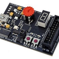
EA-EDU-009
Specifications of EA-EDU-009


Related parts for EA-EDU-009


EA-EDU-009 Summary of contents
Page 1
... The superior performance also makes these devices suitable for use as math coprocessors. Various 32-bit and 16-bit timers, an improved 10-bit ADC, PWM features through output match on all timers, and 32 fast GPIO lines with up to nine edge or level sensitive external interrupt pins make these microcontrollers particularly suitable for industrial control and medical systems ...
Page 2
... I Two 16-bit timers/external event counters with combined three capture and seven compare channels. I Low power Real-Time Clock (RTC) with independent power and dedicated 32 kHz clock input. I Multiple serial interfaces including two UARTs (16C550), two Fast I (400 kbit/s), SPI and SSP with buffering and variable data length capabilities. ...
Page 3
... FUNCTIONS system clock VECTORED INTERRUPT CONTROLLER AMBA AHB 2 I C-BUS SERIAL INTERFACES 0 AND 1 SPI AND SSP SERIAL INTERFACES UART0/UART1 REAL-TIME CLOCK SYSTEM CONTROL 002aab814 © NXP B.V. 2009. All rights reserved. (1) SCL0, SCL1 (1) SDA0, SDA1 (1) SCK0, SCK1 (1) MOSI0, MOSI1 (1) MISO0, MISO1 ...
Page 4
NXP Semiconductors 5. Pinning information 5.1 Pinning P0.19/MAT1.2/MISO1 P0.20/MAT1.3/MOSI1 P0.21/SSEL1/MAT3.0 P0.27/TRST/CAP2.0 P0.28/TMS/CAP2.1 P0.29/TCK/CAP2.2 Fig 2. LPC2101_02_03_4 Product data sheet VBAT 5 V DD(1V8) LPC2101FBD48 RST 6 LPC2102FBD48 V 7 LPC2103FBD48 XTAL1 ...
Page 5
... NXP Semiconductors P0.19/MAT1.2/MISO1 P0.20/MAT1.3/MOSI1 P0.21/SSEL1/MAT3.0 P0.27/TRST/CAP2.0 Fig 3. LPC2101_02_03_4 Product data sheet terminal 1 index area VBAT DD(1V8) LPC2102FHN48 6 RST LPC2103FHN48 LPC2103FHN48H 8 P0.28/TMS/CAP2 P0.29/TCK/CAP2.2 XTAL1 11 XTAL2 12 Transparent top view Pin configuration (HVQFN48) Rev. 04 — 2 June 2009 LPC2101/02/03 Single-chip 16-bit/32-bit microcontrollers 36 P0.11/CTS1/CAP1.1/AD0.4 35 P0.10/RTS1/CAP1.0/AD0 ...
Page 6
... Type Description I/O Port 0: Port 32-bit I/O port with individual direction controls for each bit. A total of 31 pins of the Port 0 can be used as general purpose bidirectional digital I/Os while P0. output only pin. The operation of port 0 pins depends upon the pin function selected via the pin connect block. ...
Page 7
... MAT1.0 — PWM output for Timer 1, channel 0. I AD0.5 — ADC 0, input 5. I/O P0.13 — General purpose input/output digital pin. O DTR1 — Data Terminal Ready output for UART1. O MAT1.1 — PWM output for Timer 1, channel 1. I/O P0.14 — General purpose input/output digital pin. I DCD1 — ...
Page 8
NXP Semiconductors Table 3. Pin description …continued Symbol Pin [3] P0.22/AD0.0 32 [3] P0.23/AD0.1 33 [3] P0.24/AD0.2 34 [3] P0.25/AD0.6 38 [3] P0.26/AD0.7 39 [1] P0.27/TRST/ 8 CAP2.0 [1] P0.28/TMS/ 9 CAP2.1 [1] P0.29/TCK/ 10 CAP2.2 [1] P0.30/TDI/ 15 MAT3.3 ...
Page 9
NXP Semiconductors Table 3. Pin description …continued Symbol Pin SSA V 42 DDA V 5 DD(1V8) V 17, 40 DD(3V3) VBAT 4 [ tolerant (if V and V DD(3V3) DDA [2] ...
Page 10
... It may be programmed in system via the serial port. The application program may also erase and/or program the flash while the application is running, allowing a great degree of flexibility for data storage field firmware upgrades, etc. The entire flash memory is available for user code as the bootloader resides in a separate memory. The LPC2101/02/03 fl ...
Page 11
NXP Semiconductors 6.3 On-chip static RAM On-chip static RAM may be used for code and/or data storage. The SRAM may be accessed as 8-bits, 16-bits, and 32-bits. The LPC2101/02/03 provide 2 kB static RAM. ...
Page 12
... FIQ service routine does not need to branch into the interrupt service routine but can run from the interrupt vector location. If more than one request is assigned to the FIQ class, the FIQ service routine will read a word from the VIC that identifies which FIQ source(s) is (are) requesting an interrupt. ...
Page 13
... GPIO registers. Pins may be dynamically configured as inputs or outputs. Separate registers allow setting or clearing any number of outputs simultaneously. The value of the output register may be read back, as well as the current state of the port pins. LPC2101/02/03 introduce accelerated GPIO functions over prior LPC2000 devices: • ...
Page 14
... The I C-bus is bidirectional, for inter-IC control using only two wires: a Serial Clock Line (SCL), and a Serial Data Line (SDA). Each device is recognized by a unique address and can operate as either a receiver-only device (e.g., LCD driver transmitter with the capability to both receive and send information such as serial memory. Transmitters and/or receivers can operate in either master or slave mode, depending on whether the chip has to initiate a data transfer or is only addressed ...
Page 15
... Maximum data bit rate of one eighth of the input clock rate. 6.12 SSP serial I/O controller The LPC2101/02/03 each contain one SSP. The SSP controller is capable of operation on a SPI, 4-wire SSI, or Microwire bus. It can interact with multiple masters and slaves on the bus. However, only a single master and a single slave can communicate on the bus during a given data transfer. The SSP supports full duplex transfers, with data frames of 4 bits to 16 bits fl ...
Page 16
... Do nothing on match. 6.15 Watchdog timer The purpose of the watchdog is to reset the microcontroller within a reasonable amount of time if it enters an erroneous state. When enabled, the watchdog will generate a system reset if the user program fails to ‘feed’ (or reload) the watchdog within a predetermined amount of time ...
Page 17
... T PCLK 6.16 Real-time clock The Real-Time Clock (RTC) is designed to provide a set of counters to measure time when normal or idle operating mode is selected. The RTC has been designed to use little power, making it suitable for battery powered systems where the CPU is not running continuously (Idle mode). ...
Page 18
... Power-down and Deep power-down mode, any wake-up of the processor from the Power-down modes makes use of the wake-up timer. The wake-up timer monitors the crystal oscillator as the means of checking whether it is safe to begin code execution. When power is applied to the chip, or some event caused the chip to exit Power-down mode, some time is required for the oscillator to produce a signal of suffi ...
Page 19
... IAP calls or call reinvoke ISP command to enable flash update via UART0. CAUTION If level three Code Read Protection (CRP3) is selected, no future factory testing can be performed on the device. Remark: Parts LPC2101/02/03 Revision ‘-’ have CRP2 enabled only (bootloader code version 2.2). ...
Page 20
... Power-down mode reduces chip power consumption to nearly zero. Selecting an external 32 kHz clock instead of the PCLK as a clock-source for the on-chip RTC will enable the microcontroller to have the RTC active during Power-down mode. Power-down current is increased with RTC active. However significantly lower than in Idle mode ...
Page 21
... RealMonitor RealMonitor is a configurable software module, developed by ARM Inc., which enables real time debug lightweight debug monitor that runs in the background while users debug their foreground application. It communicates with the host using the DCC, which is present in the EmbeddedICE logic. The LPC2101/02/03 contain a specific configuration of RealMonitor software programmed into the on-chip boot ROM memory ...
Page 22
... This product includes circuitry specifically designed for the protection of its internal devices from the damaging effects of excessive static charge. Nonetheless suggested that conventional precautions be taken to avoid applying greater than the rated maximum. b) Parameters are valid over operating temperature range unless otherwise specified. All voltages are with respect to V otherwise noted ...
Page 23
NXP Semiconductors 8. Static characteristics Table 5. Static characteristics +85 C for commercial applications, unless otherwise specified. amb Symbol Parameter V supply voltage DD(1V8) (1 supply voltage DD(3V3) (3 analog 3.3 ...
Page 24
... BAT current 2 I C-bus pins V HIGH-level input IH voltage V LOW-level input IL voltage V hysteresis voltage hys V LOW-level output OL voltage I input leakage LI current Oscillator pins V input voltage on pin i(XTAL1) XTAL1 LPC2101_02_03_4 Product data sheet …continued Conditions [12] V < V < DD(3V3) I Active mode; code while(1){} executed from fl ...
Page 25
... DDA Conditions = 3.3 V for 10-bit resolution at full speed; V DD(3V3 the difference between the actual step width and the ideal step width. See ) is the peak difference between the center of the steps of the actual and the ideal transfer curve after Figure 5. Figure Figure 5. Rev. 04 — ...
Page 26
... E O (1) Example of an actual transfer curve. (2) The ideal transfer curve. (3) Differential linearity error (E (4) Integral non-linearity (E L(adj) (5) Center of a step of the actual transfer curve. Fig 5. ADC conversion characteristics LPC2101_02_03_4 Product data sheet (2) (5) (4) (3) 1 LSB (ideal) 1018 4 5 ...
Page 27
... Test conditions: Deep power-down mode entered 3.3 V. DD(3V3) DDA Battery supply current I measured at different temperatures and conditions BAT Rev. 04 — 2 June 2009 LPC2101/02/03 Single-chip 16-bit/32-bit microcontrollers 002aae680 V =1.8 V DD(1V8) 1 Temperature ( C) 002aae681 RTC on; SRAM on RTC on; SRAM off RTC off ...
Page 28
... Test conditions: Deep power-down mode entered; RTC off; SRAM off 1 3.3 V. DD(1V8) i(BAT) DDA I/O supply current I measured at different temperatures DD(IO) Rev. 04 — 2 June 2009 LPC2101/02/03 Single-chip 16-bit/32-bit microcontrollers 002aae682 35 60 Temperature ( C) = 3.3 V; DD(3V3) © NXP B.V. 2009. All rights reserved. ...
Page 29
NXP Semiconductors 9. Dynamic characteristics Table 7. Dynamic characteristics for commercial applications +85 C for industrial applications, V amb [1] specified ranges . Symbol Parameter External clock f oscillator frequency ...
Page 30
... Loops must be made as small as possible, in order to keep the noise coupled in via the PCB as small as possible. Also parasitics should stay as small as possible. Values of C smaller accordingly to the increase in parasitics of the PCB layout. LPC2101_02_03_4 Product data sheet Single-chip 16-bit/32-bit microcontrollers Rev. 04 — ...
Page 31
... NXP Semiconductors 11. Package outline LQFP48: plastic low profile quad flat package; 48 leads; body 1 pin 1 index DIMENSIONS (mm are the original dimensions) A UNIT max. 0.20 1.45 1.6 mm 0.25 0.05 1.35 Note 1. Plastic or metal protrusions of 0.25 mm maximum per side are not included. OUTLINE VERSION ...
Page 32
... NXP Semiconductors HVQFN48: plastic thermal enhanced very thin quad flat package; no leads; 48 terminals; body 0.85 mm terminal 1 index area terminal 1 48 index area DIMENSIONS (mm are the original dimensions) (1) A UNIT max 0.05 0. 0.2 0.00 0.18 Note 1. Plastic or metal protrusions of 0.075 mm maximum per side are not included ...
Page 33
... NXP Semiconductors HVQFN48: plastic thermal enhanced very thin quad flat package; no leads; 48 terminals; body 0.85 mm terminal 1 index area terminal 1 48 index area DIMENSIONS (mm are the original dimensions) (1) A UNIT max 0.05 0. 0.2 0.00 0.15 Note 1. Plastic or metal protrusions of 0.075 mm maximum per side are not included ...
Page 34
NXP Semiconductors 12. Abbreviations Table 8. Acronym ADC AMBA APB DCC DSP FIFO FIQ GPIO IAP IRQ ISP PLL PWM SPI SRAM SSI SSP TTL UART VIC LPC2101_02_03_4 Product data sheet Acronym list Description Analog-to-Digital Converter Advanced Microcontroller Bus Architecture ...
Page 35
... Table 9. Revision history Document ID Release date LPC2101_02_03_4 20090602 • Modifications: Section 6.17.4 “Code security (Code Read Protection - CRP levels (applicable to Revision A and higher). • Section 6.17.7 “Power Revision A and higher). • Section 10.1 “XTAL1 input” • Section 10.2 “XTAL and RTC Printed Circuit Board (PCB) layout guidelines” ...
Page 36
... Qualification Product [short] data sheet Production [1] Please consult the most recently issued document before initiating or completing a design. [2] The term ‘short data sheet’ is explained in section “Definitions”. [3] The product status of device(s) described in this document may have changed since this document was published and may differ in case of multiple devices. The latest product status information is available on the Internet at URL http://www.nxp.com. 14.2 Defi ...
Page 37
... NXP Semiconductors 16. Contents 1 General description . . . . . . . . . . . . . . . . . . . . . . 1 2 Features . . . . . . . . . . . . . . . . . . . . . . . . . . . . . . . 1 2.1 Enhanced features . . . . . . . . . . . . . . . . . . . . . . 1 2.2 Key features . . . . . . . . . . . . . . . . . . . . . . . . . . . 1 3 Ordering information . . . . . . . . . . . . . . . . . . . . . 2 3.1 Ordering options . . . . . . . . . . . . . . . . . . . . . . . . 2 4 Block diagram . . . . . . . . . . . . . . . . . . . . . . . . . . 3 5 Pinning information . . . . . . . . . . . . . . . . . . . . . . 4 5.1 Pinning . . . . . . . . . . . . . . . . . . . . . . . . . . . . . . . 4 5.2 Pin description . . . . . . . . . . . . . . . . . . . . . . . . . 6 6 Functional description . . . . . . . . . . . . . . . . . . 10 6.1 Architectural overview 6.2 On-chip flash program memory . . . . . . . . . . . 10 6 ...